News Posts matching #TSMC

Return to Keyword Browsing

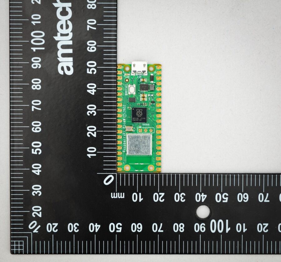
The Raspberry Pi Foundation Launches the $6 Raspberry Pi Pico W

New product alert! In January last year, we launched the $4 Raspberry Pi Pico, our first product built on silicon designed here at Raspberry Pi. At its heart is the RP2040 microcontroller, built on TSMC's 40 nm low-power process, and incorporating two 133 MHz Arm Cortex-M0+ cores, 264kB of on-chip SRAM, and our unique programmable I/O subsystem. Since launch, we've sold nearly two million Pico boards, and RP2040 has found its way into a huge number of third-party products. We always believed that RP2040 was a great fit for commercial and industrial applications, but the global semiconductor shortage has vastly accelerated adoption. With millions of units on hand today, and pipeline in place for tens of millions more, design engineers who have been let down by their current suppliers have a perfect excuse to experiment.

Fast cores, large memory, and flexible interfacing make RP2040 a natural building block for Internet of Things (IoT) applications. But Pico itself has one obvious missing feature for IoT: a method for connecting to the network. Now, this is about to change. Today, we're launching three new members of the Pico family. Raspberry Pi Pico W is priced at $6, and brings 802.11n wireless networking to the Pico platform, while retaining complete pin compatibility with its older sibling. Pico H ($5) and Pico WH ($7) add pre-populated headers, and our new 3-pin debug connector, to Pico and Pico W respectively. Pico H and Pico W are available today; Pico WH will follow in August.

TSMC Expected to be Affected by Increased Electricity Costs in Taiwan

The island of Taiwan is in many ways very much still stuck in an era where the government controls most utilities and where there is little to no competition. For example, the government controls fuel prices, be that for your motor vehicle or for cooking and heating. This also applies to the cost of electricity in most cases and the Ministry of Economic Affairs has announced that the electricity price will increase by up to 15 percent for high usage customers, which translates to the industry. The increase might sound tiny at just over 1.3 cents per kilowatt hour, for a total cost of 10.43 cents per kWh. However, a company like TSMC that uses a lot of electricity, is expected to see an increase in costs of at least US$135 million per year, according to some Taiwanese news sources, while others claim it'll be as much as US$270 million.

TSMC does in all fairness produce some of its own electricity thanks to solar panels on many of its buildings and the company has also invested heavily in renewable energy. In fact, TSMC has bought up almost all available renewable capacity in Taiwan and the company is committed to using 100 percent renewable energy in the long term. Currently a mere 8 percent (based on 2020 estimates) is coming from TSMC's own efforts, but the company should be at somewhere around 12-15 percent overall. Even so, these extra costs are likely to be reflected in future customer pricing. It's the first price hike in four years, but as Taiwan is a manufacturing nation, TSMC is unlikely to be the only company affected, but the price hike is related to global inflation and is targeting high-usage businesses and consumers alike.

GlobalWafers Selects Sherman, Texas for New Semiconductor Silicon Wafer Site

Hsinchu, Taiwan-based global semiconductor silicon wafer company, GlobalWafers, announced today that it plans to build a state-of-the-art 300-millimeter silicon wafer factory in Sherman, Texas, which is the first of its kind in the USA over twenty (20) years. Construction is expected to commence later this year. This 300-millimeter greenfield investment is consistent with the Company's announcement on February 6th of this year of brownfield and greenfield expansions totaling NTD 100 bn. This new Texas investment could also support as many as 1,500 jobs with production volumes ultimately reaching 1.2 mn wafers per month after multiple stages of equipment installation, in alignment with market demand.

300-millimeter silicon wafers are the starting material for all advanced semiconductor fabrication sites (or fabs), including recently announced United States (US) expansions by GlobalFoundries, Intel, Samsung, Texas Instruments and TSMC. Most of these wafers are currently manufactured in Asia, forcing the US semiconductor industry to highly rely on imported silicon wafers. This investment will represent the first new silicon wafer facility in the US in over two decades and close a critical semiconductor supply chain gap.

Off-season Offsets Wafer Pricing Increase, 1Q22 Foundry Output Value Up 8.2% QoQ, Says TrendForce

According to TrendForce research, although demand for consumer electronics remains weak, structural growth demand in the semiconductor industry including for servers, high-performance computing, automotive, and industrial equipment has not flagged, becoming a key driver for medium and long term foundry growth. At the same time, due to robust wafer production at higher pricing in 1Q22, quarterly output value hit a new high for the 11th consecutive quarter, reaching US$31.96 billion, 8.2% QoQ, marginally less than the previous quarter. In terms of ranking, the biggest change is Nexchip surpassed Tower at the ninth position.

TSMC's across the board wafer hikes in 4Q21 on batches primarily produced in 1Q22 coupled with sustained strong demand for high-performance computing and better foreign currency exchange rates pushed TSMC's 1Q22 revenue to $17.53 billion, up 11.3% QoQ. Quarterly revenue growth by node was generally around 10% and the 7/6 nm and 16/12 nm processes posted the highest growth rate due to small expansions in production. The only instance of revenue decline came at the 5/4 nm process due to Apple's iPhone 13 entering the off season for production stocking.

Cadence Achieves PCIe 5.0 Specification Compliance for PHY and Controller IP in TSMC Advanced Technologies

Cadence Design Systems, Inc. (Nasdaq: CDNS) today announced that its PHY and Controller IP for the PCI Express (PCIe ) 5.0 specification in the TSMC N7, N6 and N5 process technologies have passed certification tests from PCI-SIG at the industry's first event for PCIe 5.0 specification compliance held in April. The Cadence solutions were tested to their full potential and complied with the full speed of 32GT/s for PCIe 5.0 technology. The compliance program provides designers with testing procedures to assess that the PCIe 5.0 interfaces on their system-on-chip (SoC) designs will operate as expected.

The Cadence IP for PCIe 5.0 technology consists of a PHY, companion controller and Verification IP (VIP) targeted at SoC designs for very high-bandwidth hyperscale computing, networking and storage applications. With Cadence's PHY and Controller Subsystem for PCIe 5.0 architecture, customers can design extremely power-efficient SoCs while accelerating time to market.

AMD "Phoenix Point" Zen 4 Mobile Processor Powered Up

An engineering sample of AMD's next-generation Ryzen "Phoenix Point" mobile processor has been powered up, and made its first appearance on the Geekbench user-database. "Phoenix Point" is a monolithic silicon mobile processor built on the TSMC N5 (5 nm EUV) process, featuring "Zen 4" CPU cores, and a significantly faster iGPU based on the RDNA3 graphics architecture; along with a DDR5/LPDDR5 memory interface, and PCI-Express Gen 5.0 capability. An engineering sample with an 8-core/16-thread CPU, with the OPN code "100-000000709-23_N," hit the radar. AMD could debut Ryzen "Phoenix Point" in the first quarter of 2023, possibly with an International CES announcement.

TSMC Announces the N3 FinFlex, N3E, and N2 Nodes, and 3DFabric

TSMC today showcased the newest innovations in its advanced logic, specialty, and 3D IC technologies at the Company's 2022 North America Technology Symposium, with the next-generation leading-edge N2 process powered by nanosheet transistors and the unique FINFLEX technology for the N3 and N3E processes making their debut.

Resuming as an in-person event after being held online in the past two years, the North America symposium in Santa Clara, California, kicks off a series of Technology Symposiums around the world in the coming months. The Symposiums also feature an Innovation Zone that spotlights the achievements of TSMC's emerging start-up customers.

Intel Arc A380 Desktop Graphics Card Launched in China at $153 (equivalent)

Intel officially launched the Arc A380 "Alchemist" entry-mainstream desktop graphics card in China, priced at RMB ¥1,030, including VAT, which roughly converts to USD $153. The Arc A380 "Alchemist" is based on the Xe-HPG graphics architecture, and the smaller DG2-128 (ACM-G11) silicon, which is built on the TSMC N6 (6 nm) silicon fabrication process.

The A380 desktop GPU is endowed with 8 Xe Cores, or 128 EU (execution units), which work out to 1,024 unified shaders. The chip features a 96-bit wide GDDR6 memory interface, running 6 GB of memory. Despite these hardware specs, you get full DirectX 12 Ultimate capability, including ray tracing, and the XeSS performance enhancement. There are also several content-creation accelerators, including Intel XMX, and AV1 hardware-encode capabilities.

AMD Ryzen 3 7320U Surfaces, Possibly the "Mendocino" SoC

One of AMD's big announcements this fall has been its entry-level "Mendocino" Ryzen 3 mobile processor, which enables the company to compete with Intel's latest-generation Pentium Gold-powered notebooks by combining older-generation IP with the latest I/O and fabrication node. The chip has possibly surfaced on the UserBenchmark database, as the Ryzen 3 7320U processor.

Built on the TSMC N6 (6 nm) silicon fabrication process, the "Mendocino" chip features a 4-core/8-thread CPU based on the older "Zen 2" microarchitecture. This CPU is a single CCX with four "Zen 2" cores sharing a 4 MB L3 cache. It features an iGPU based on the latest RDNA2 graphics architecture, but with just two compute units (128 stream processors). The chip also features a single-channel DDR5 memory interface, and a PCI-Express Gen 3 interface with four PCIe 3.0 general-purpose lanes, besides some USB and display outputs.

AMD Plans Late-October or Early-November Debut of RDNA3 with Radeon RX 7000 Series

AMD is planning to debut its next-generation RDNA3 graphics architecture with the Radeon RX 7000 series desktop graphics cards, some time in late-October or early-November, 2022. This, according to Greymon55, a reliable source with AMD and NVIDIA leaks. We had known about a late-2022 debut for AMD's next-gen graphics, but now we have a finer timeline.

AMD claims that RDNA3 will repeat the feat of over 50 percent generational performance/Watt gains that RDNA2 had over RDNA. The next-generation GPUs will be built on the TSMC N5 (5 nm EUV) silicon fabrication process, and debut a multi-chip module design similar to AMD's processors. The logic dies with the GPU's SIMD components will be built on the most advanced node, while the I/O and display/media accelerators will be located in separate dies that can make do on a slightly older node.

Cadence Digital and Custom/Analog Design Flows Certified by TSMC for Latest N3E and N4P Processes

Cadence Design Systems, Inc. today announced that its digital and custom/analog design flows have been certified for the TSMC N3E and N4P processes, supporting the latest Design Rule Manual (DRM). In addition, Cadence and TSMC delivered N3E and N4P process design kits (PDKs) and design flows to accelerate customer adoption and advance mobile, AI and hyperscale computing design innovation. Joint customers are actively designing with the new N3E and N4P PDKs, and several test chips have already been taped out, which demonstrates how Cadence solutions help customers improve engineering efficiency and maximize the power, performance and area (PPA) benefits offered by the latest TSMC process technologies. The Cadence digital and custom/analog advanced-node solutions support the company's Intelligent System Design strategy, enabling system-on-chip (SoC) design excellence.

Cadence worked closely with TSMC to ensure the digital full flow was optimized for TSMC's advanced N3E and N4P process technologies. The complete RTL-to-GDS flow includes the Cadence Innovus Implementation System, Quantus Extraction Solution, Quantus Field Solver, Tempus Timing Signoff Solution and ECO option, Pegasus Verification System, Liberate Characterization Solution and Voltus IC Power Integrity Solution. Additionally, the Cadence Genus Synthesis Solution and predictive iSpatial technology are enabled for the TSMC N3E and N4P process technologies.

AMD Said to Become TSMC's Third Largest Customer in 2023

Based on a report in the Taiwanese media, AMD is quickly becoming a key customer for TSMC and is expected to become its third largest customer in 2023. This is partially due to new orders that AMD has placed with TSMC for its 5 nm node. AMD is said to become TSMC's single largest customer for its 5 nm node in 2023, although it's not clear from the report how large of a share of the 5 nm node AMD will have.

The additional orders are said to be related to AMD's Zen 4 based processors, as well as its upcoming RDNA3 based GPUs. AMD is expected to be reaching a production volume of some 20,000 wafers in the fourth quarter of 2022, although there's no mention of what's expected in 2023. Considering most of AMD's products for the next year or two will all be based on TSMC's 5 nm node, this shouldn't come as a huge surprise though, as AMD has a wide range of new CPU and GPU products coming.

Intel "Meteor Lake-P" SoC with 6P+8E Compute Tile Pictured

Intel's next-generation "Meteor Lake-P" mobile processor with a 6P+8E Compute Tile was shown off at the 2022 IEEE VLSI Symposium on Tech and Circuits (6 performance cores and 8 efficiency cores). We now have annotations for all four tiles, as well as a close-up die-shot of the Compute Tile. Intel also confirmed that the Compute Tile will be built on its homebrew Intel 4 silicon fabrication process, which offers over 20% iso-power performance increase versus the Intel 7 node, through extensive use of EUV lithography.

We had earlier seen a 2P+8E version of the "Meteor Lake" Compute Tile, probably from the "Meteor Lake-U" package. The larger 6P+8E Compute tile features six "Redwood Cove" performance cores, and two "Crestmont" efficiency core clusters, each with four E-cores. Assuming the L3 cache slice per P-core or E-core cluster is 2.5 MB, there has to be 20 MB of L3 cache on the compute tile. Each P-core has 2 MB of dedicated L2 cache, while each of the two E-core clusters shares 4 MB of L2 cache among four E-cores.

TSMC Forecasts 30 Percent Increase in Sales for 2022

In 2021 TSMC saw an increase in sales of 24.9 percent in monetary value, but for 2022, the company is expecting this figure to reach somewhere around the 30 percent mark. For this quarter alone, TSMC is expecting a revenue of somewhere between US$17.6 to US$18.2 billion, with a gross margin ending up as high as 58 percent. Despite the positive outlook, TSMC hasn't been doing well on the Taiwanese stock exchange this year, as the company has lost more than a tenth of its value in 2022.

That said, TSMC is pressing forward and will still be spending in excess of US$40 billion in 2023 to expand its production capacity, following the US$40 to US$44 billion it will invest this year. The company isn't overly concerned about inflation at this point in time either, saying it doesn't have a direct impact on the semiconductor industry. TSMC is seeing a slowdown in the consumer chip space, but it's seeing an uptick in business when it comes to EV related ICs. TSMC's production lines are at full utilisation for at least the rest of 2022, but most likely long into 2023.

After TSMC, Intel May be Edging Closer to Samsung for Collaboration

Intel's revamped IDM 2.0 strategy has seen the company revise its stance in both in-house and outsourced silicon fabrication. While we're already seeing the fruits of Intel's collaboration with TSMC (albeit at the relatively slow pace of introduction for Intel's Arc Alchemist graphics), it seems that Intel is willing to go much farther than just TSMC as a source of chips for its product portfolio.

That's the backdrop to which Intel CEO Pat Gelsinger recently took a trip to South Korea's capital of Seoul. According to the Korea Herald, Gelsinger met several key Samsung executives, including Samsung Electronics Vice Chairman Lee Jae-yong, co-CEO and chip business boss Kyung Kye-hyun, and head of Samsung Mobile Roh Tae-moon. More than enough executive grunt to ignite talks of a deepening collaboration between both companies. While the reporting source doesn't provide any quotes or actionable intel from the meeting, Samsung remains one of the key semiconductor manufacturers alongside Intel itself and TSMC, with a particularly strong portfolio in memory-related technologies.

Phison Showcases 12 GB/s Speeds for PCIe 5.0 SSDs Through Its New E26 Controller

Phison has showcased the expected performance of its upcoming PS5026-E26 controller, built to usher NVMe SSDs into the PCIe 5.0 realm. The company showcased its new controller's prowess by building a reference SSD design based on 1 TB of Micron's TLC NAND. Phison's new controller has been built from the ground-up to accelerate next-generation SSD workloads - including direct access technologies based on Microsoft's DirectStorage API, accelerated by two ARM Cortex-R5 cores and three proprietary CoXProcessor 2.0 accelerators built on TSMC's 12 nm process.

Phison's internal testing shows its reference SSD achieving sequential read speeds of over 12 GB/s in CrystalDiskMark, with sequential writes going as high as 10 GB/s - a 70% performance increase compared to the world's fastest PCIe 4.0 SSDs, which currently top out at around 7 GB/s sequential speeds. As to 4K performance, one of the most tangible metrics for user experience, random reads are set at around 16.000 IOPS, showcasing room for improvement with further firmware optimizations for actual shipping products.

TSMC Said to be Eyeing Singapore for Fab Expansion

The rumour mill never seems to stop churning when it comes to TSMC and now the company is said to be looking at the tiny nation of Singapore for a future fab. This time the information comes via the Wall Street Journal rather than the usual Taiwanese sources and although the publication points out that no decision has been made at this point in time, it says that TSMC is apparently in talks with the Economic Development Board of Singapore. The official statement from the TSMC on the matter is that the company "doesn't rule out any possibility but does not have any concrete plan at this time".

The potential Singapore Fab would be producing 28 to 7 nm chips, in other words, quite far from TSMC's cutting edge nodes. However, TSMC is already building a similar facility in the southern city of Kaohsiung in Taiwan that's scheduled for opening in 2024. As such, the nodes used in a future facility in Singapore might change depending on when the fab will open and it might end up producing chips on more advanced nodes as well. As these fabs take a few years to get going, they're not projects that are started on a whim. We should also mention that TSMC already has a joint venture in Singapore together with NXP, called SSMC, which also produces for third parties.

NVIDIA Releases Security Update 473.47 WHQL Driver for Kepler GPUs

Ten years ago, in 2012, NVIDIA introduced its Kepler series of graphics cards based on the TSMC 28 nm node. Architecture has been supported for quite a while now by NVIDIA's drivers, and the last series to carry support was the 470 driver class. Today, NVIDIA pushed a security update in the form of a 473.47 WHQL driver that brings fixes to various CVE vulnerabilities that can cause anything from issues that may lead to denial of service, information disclosure, or data tampering. This driver version has no fixed matters and doesn't bring any additional features except the fix for vulnerabilities. With CVEs rated from 4.1 to 8.5, NVIDIA has fixed major issues bugging Kepler GPU users. With a high risk for code execution, denial of service, escalation of privileges, information disclosure, and data tampering, the 473.47 WHQL driver is another step for supporting Kepler architecture until 2024, when NVIDIA plans to drop the support for this architecture. Supported cards are GT 600, GT 700, GTX 600, GTX 700, Titan, Titan Black, and Titan Z.

The updated drivers are available for installation on NVIDIA's website and for users of TechPowerUp's NVCleanstall software.

NVIDIA GeForce RTX 4090 Twice as Fast as RTX 3090, Features 16128 CUDA Cores and 450W TDP

NVIDIA's next-generation GeForce RTX 40 series of graphics cards, codenamed Ada Lovelace, is shaping up to be a powerful graphics card lineup. Allegedly, we can expect to see a mid-July launch of NVIDIA's newest gaming offerings, where customers can expect some impressive performance. According to a reliable hardware leaker, kopite7kimi, NVIDIA GeForce RTX 4090 graphics card will feature AD102-300 GPU SKU. This model is equipped with 126 Streaming Multiprocessors (SMs), which brings the total number of FP32 CUDA cores to 16128. Compared to the full AD102 GPU with 144 SMs, this leads us to think that there will be an RTX 4090 Ti model following up later as well.

Paired with 24 GB of 21 Gbps GDDR6X memory, the RTX 4090 graphics card has a TDP of 450 Watts. While this number may appear as a very power-hungry design, bear in mind that the targeted performance improvement over the previous RTX 3090 model is expected to be a two-fold scale. Paired with TSMC's new N4 node and new architecture design, performance scaling should follow at the cost of higher TDPs. These claims are yet to be validated by real-world benchmarks of independent tech media, so please take all of this information with a grain of salt and wait for TechPowerUp reviews once the card arrives.

Intel "Meteor Lake" 2P+8E Silicon Annotated

Le Comptoir du Hardware scored a die-shot of a 2P+8E core variant of the "Meteor Lake" compute tile, and Locuza annotated it. "Meteor Lake" will be Intel's first processor to implement the company's IDM 2.0 strategy to the fullest. The processor is a multi-chip module of various tiles (chiplets), each with a certain function, sitting on die made on a silicon fabrication node most suitable to that function. Under this strategy, for example, if Intel's chip-designers calculate that the iGPU will be the most power-hungry component on the processor, followed by the CPU cores, the graphics tile will be built on a more advanced process than the compute tile. Intel's "Meteor Lake" and "Arrow Lake" processors will implement chiplets built on the Intel 4, TSMC N3, and Intel 20A fabrication nodes, each with unique power and transistor-density characteristics. Learn more about the "Meteor Lake" MCM in our older article.

The 2P+8E (2 performance cores + 8 efficiency cores) compute tile is one among many variants of compute tiles Intel will develop for the various SKUs making up the next-generation Core mobile processor series. The die is annotated with the two large "Redwood Cove" P-cores and their cache slices taking up about 35% of the die area; and the two "Crestmount" E-core clusters (each with 4 E-cores), and their cache slices, taking up the rest. The two P-cores and two E-core clusters are interconnected by a Ring Bus, and share an L3 cache. The size of each L3 cache slice is either 2.5 MB or 3 MB. At 2.5 MB, the total L3 cache will be 10 MB, and at 3 MB, it will be 12 MB. As with all past generations, the L3 cache is fully accessible by all CPU cores in the compute tile.

TSMC Said to be Planning Price Increases in 2023

The global inflation rises are no secret and more and more companies are looking to increase prices of their goods, so not entirely unsurprising, reports of TSMC planning price hikes in early 2023 are starting to appear. TSMC has supposedly already contacted its customers to notify them about the upcoming price increase, to give them as much time as possible to make any changes to their plans, if needed. The price increase will vary depending on the node in question, but is reported to be somewhere between five and eight percent according to the Nikkei.

Part of the increase is also related to TSMC's rapid expansion that's going on at the moment, since the company is going to need to invest a lot more capital when it comes to building the advanced fabs that its customers are relying on. TSMC is expected to invest some US$40-44 billion this year alone on fabs and new equipment. This is a fairly small price increase compared to the big increase TSMC implemented in August 2021, where some nodes saw price hikes of up to 20 percent. That said, TSMC isn't alone in increasing their pricing, as UMC and SMIC have also increased their prices several times since last year. Nikkei claims that UMC and SMIC are charging more than TSMC on some nodes. However, in the past, TSMC used to offer discounts to its clients on a quarterly basis once a chip had gone into mass production and everything progressed smoothly, but TSMC discontinued this discount scheme last year. As such, it looks like cheaper chip costs aren't to be expected any time soon.

AMD Ryzen 7000U "Phoenix" Processor iGPU Matches RTX 3060 Laptop GPU Performance: Rumor

AMD is planning a massive integrated graphics performance uplift for its next-generation Ryzen 7000U mobile processors. Codenamed "Phoenix," this SoC will feature a CPU based on the "Zen 4" microarchitecture with a higher CPU core count than the Intel alternative of the time; and an iGPU based on the RDNA3 graphics architecture. AMD is planning to endow this with the right combination of a CU count and engine clocks, to result in performance that roughly matches the NVIDIA GeForce RTX 3060 Laptop GPU, a popular performance-segment discrete GPU for notebooks, according to greymon55. Other highlights of "Phoenix" include a DDR5 + LPDDR5 memory interface, and PCI-Express Gen 5. The SoC is expected to be built on the TSMC N5 (5 nm) process, and debut in 2023.

NVIDIA H100 SXM Hopper GPU Pictured Up Close

ServeTheHome, a tech media outlet focused on everything server/enterprise, posted an exclusive set of photos of NVIDIA's latest H100 "Hopper" accelerator. Being the fastest GPU NVIDIA ever created, H100 is made on TSMC's 4 nm manufacturing process and features over 80 billion transistors on an 814 mm² CoWoS package designed by TSMC. Complementing the massive die, we have 80 GB of HBM3 memory that sits close to the die. Pictured below, we have an SXM5 H100 module packed with VRM and power regulation. Given that the rated TDP for this GPU is 700 Watts, power regulation is a serious concern and NVIDIA managed to keep it in check.

On the back of the card, we see one short and one longer mezzanine connector that acts as a power delivery connector, different from the previous A100 GPU layout. This board model is labeled PG520 and is very close to the official renders that NVIDIA supplied us with on launch day.

NVIDIA Hopper Whitepaper Reveals Key Specs of Monstrous Compute Processor

The NVIDIA GH100 silicon powering the next-generation NVIDIA H100 compute processor is a monstrosity on paper, with an NVIDIA whitepaper published over the weekend revealing its key specifications. NVIDIA is tapping into the most advanced silicon fabrication node currently available from TSMC to build the compute die, which is TSMC N4 (4 nm-class EUV). The H100 features a monolithic silicon surrounded by up to six on-package HBM3 stacks.

The GH100 compute die is built on the 4 nm EUV process, and has a monstrous transistor-count of 80 billion, a nearly 50% increase over the GA100. Interestingly though, at 814 mm², the die-area of the GH100 is less than that of the GA100, with its 826 mm² die built on the 7 nm DUV (TSMC N7) node, all thanks to the transistor-density gains of the 4 nm node over the 7 nm one.

NVIDIA AD102 and AMD Navi 31 in a Race to Reach 100 TFLOPs FP32 First

A technological race is brewing between NVIDIA and AMD over which brand's GPU reaches the 100 TFLOP/s peak FP32 throughput mark first. AMD's TeraScale graphics architecture and the "RV770" silicon, were the first to hit the 1 TFLOP/s mark, way back in 2008. It would take 14 years for this figure to reach 100 TFLOP/s for flagship GPUs. NVIDIA's next generation big GPU based on the "Ada Lovelace," the AD102, is the green team's contender for the 100 TFLOP/s mark, according to kopite7kimi. To achieve this, all 144 streaming multiprocessors (SM) or 18,432 CUDA cores, of the AD102 will have to be enabled.

From the red team, the biggest GPU based on the next-generation RDNA3 graphics architecture, "Navi 31," could offer peak FP32 throughput of 92 TFLOP/s according to greymon55, which gives AMD the freedom to create special SKUs running at high engine clocks, just to reach the 100 TFLOP/s mark. The Navi 31 silicon is expected to triple the compute unit count over its predecessor, resulting in 15,360 stream processors. Both the AD102 and Navi 31 are expected to be built on the same TSMC N5 (5 nm EUV) node, and product launches for both are expected by year-end.
Return to Keyword Browsing
Feb 16th, 2025 17:50 EST change timezone

New Forum Posts

Popular Reviews

Controversial News Posts