Report Suggests German Government Prepping $22 Billion Aid Package for Native Chip Production
According to a report published by Bloomberg, the German government has formed plans to create €20 billion ($22 billion) of investments to aid in the growth of local semiconductor manufacturing. The article proposes that the organization is racing to bolster the country's technology sector, and is attempting to secure essential supplies of components. Various geopolitical issues have complicated matters in recent times. Funding will be made available to German and international companies, from Germany's (now diversified) Climate and Transformation reserve, over the next four years. The finance ministry responded to Bloomberg's query, and stated: "The draft for the economic plan 2024 and the financial plan until 2027 for the Climate and Transformation Fund are currently being prepared...This process has not yet been completed." Germany's economy ministry did not provide a statement/response to Bloomberg's queries.
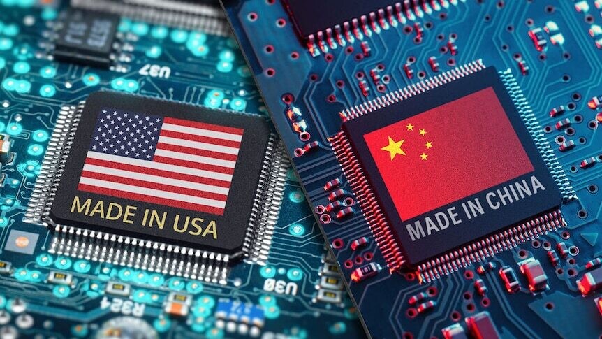
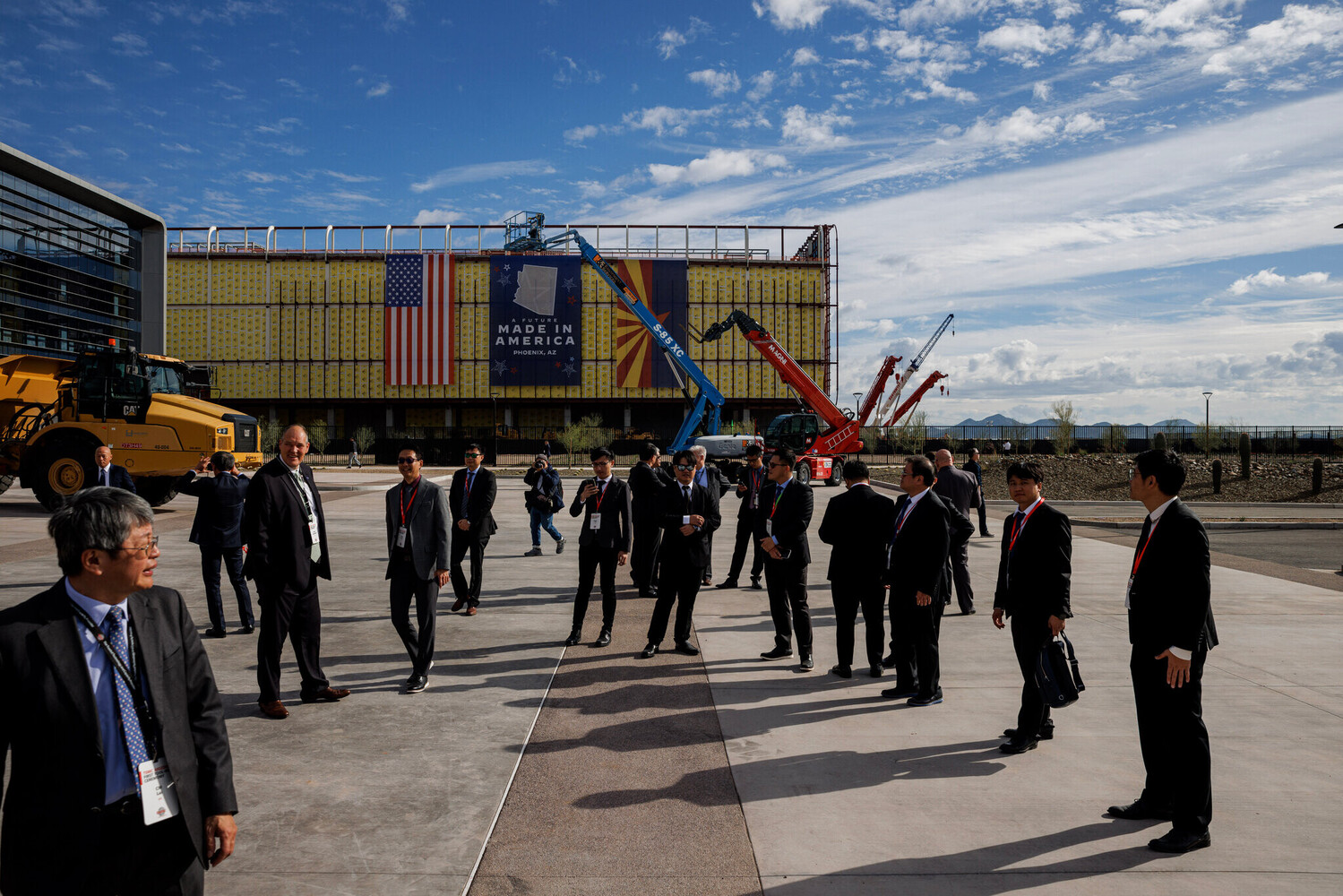
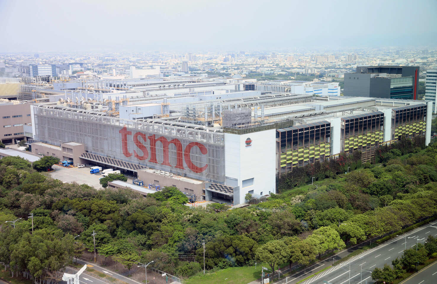
Around 75% of the fund is reportedly set aside for multinational semiconductor firms including Intel Corporation (USA) and Taiwan Semiconductor Manufacturing Company Limited (TSMC). Bloomberg believes that Team Blue is due an allocation of €10 billion for investments in its new production facility, located close to Magdeburg, Germany. The government is allegedly deep into talks with TSMC regarding the foundation of a proposed €10 billion production base in the Dresden area—the likes of BMW, Mercedes-Benz and Volkswagen AG would benefit greatly with quicker access to (localized) microcontrollers manufacturing facilities. The government could subsidize half of that total investment (€5 billion). Infineon is possibly in line to receive a €1 billion aid package, since it is building a new fab location in Dresden.

Around 75% of the fund is reportedly set aside for multinational semiconductor firms including Intel Corporation (USA) and Taiwan Semiconductor Manufacturing Company Limited (TSMC). Bloomberg believes that Team Blue is due an allocation of €10 billion for investments in its new production facility, located close to Magdeburg, Germany. The government is allegedly deep into talks with TSMC regarding the foundation of a proposed €10 billion production base in the Dresden area—the likes of BMW, Mercedes-Benz and Volkswagen AG would benefit greatly with quicker access to (localized) microcontrollers manufacturing facilities. The government could subsidize half of that total investment (€5 billion). Infineon is possibly in line to receive a €1 billion aid package, since it is building a new fab location in Dresden.