News Posts matching #TSMC

Return to Keyword Browsing

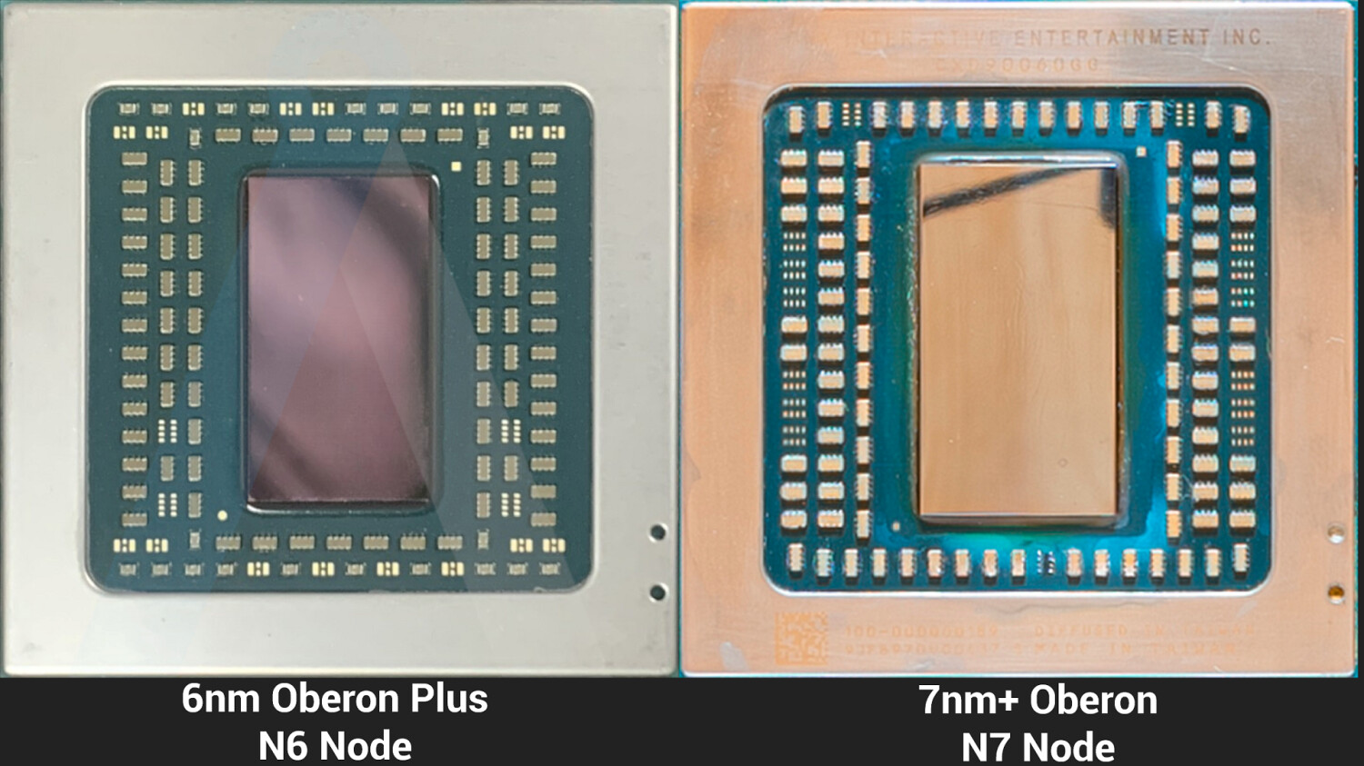
Eliyan Closes $40M Series A Funding Round and Unveils Industry's Highest Performance Chiplet Interconnect Technologies

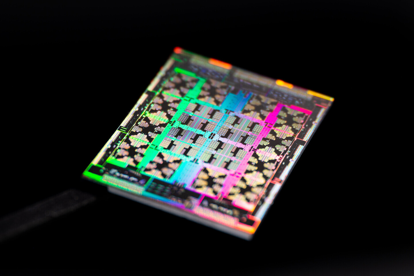
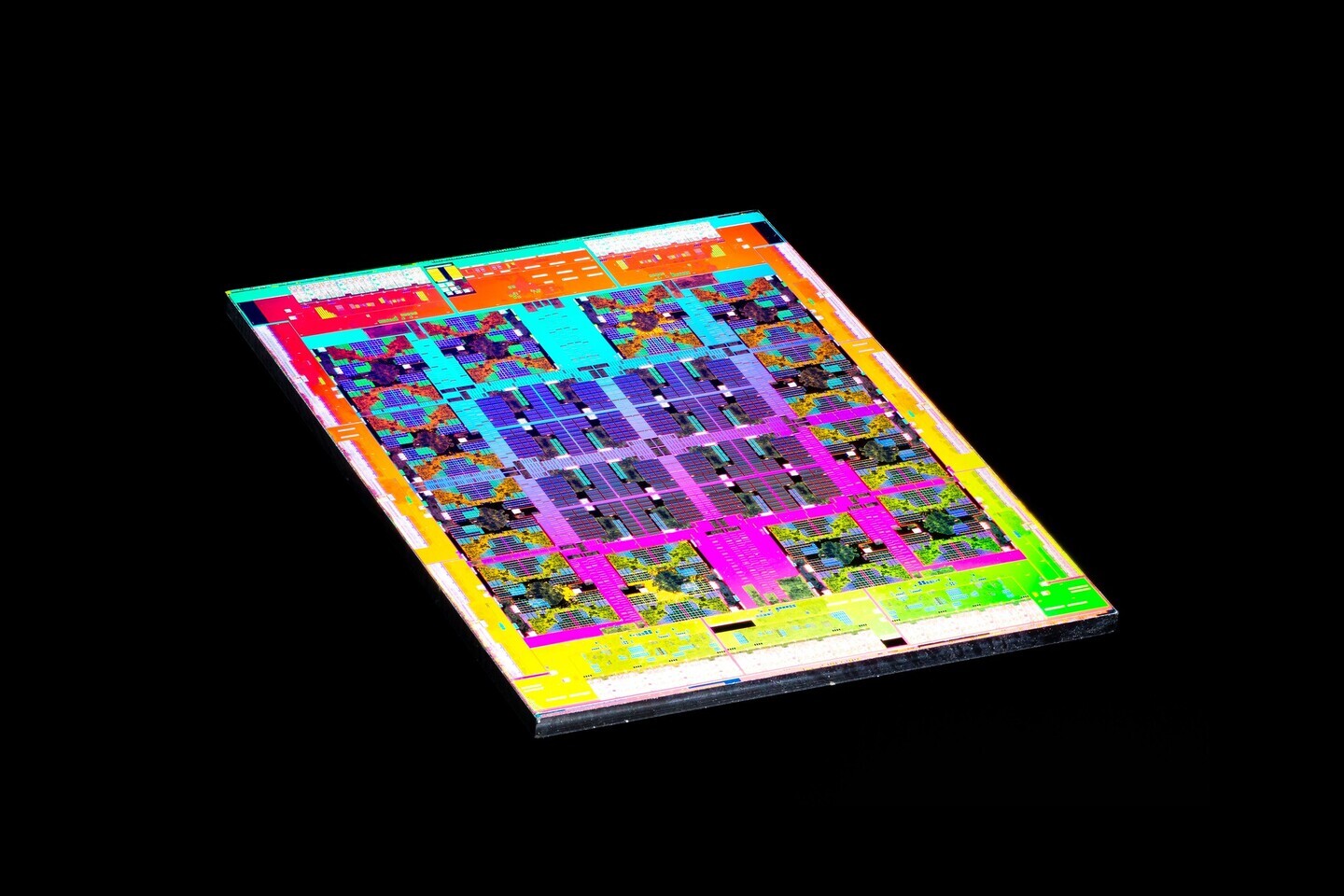
Eliyan Corporation, credited for the invention of the semiconductor industry's highest-performance and most efficient chiplet interconnect, today announced two major milestones in the commercialization of its technology for multi-die chiplet integration: the close of its Series A $40M funding round, and the successful tapeout of its technology on an industry standard 5-nanometer (nm) process.

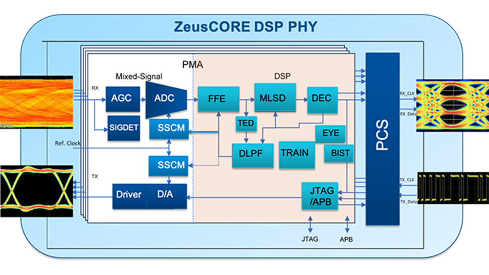
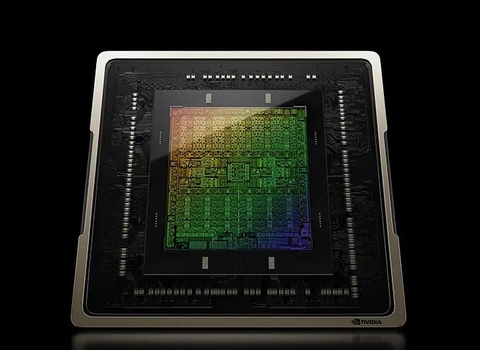
Eliyan's NuLink PHY and NuGear technologies address the critical need for a commercially viable approach to enabling high performance and cost-effectiveness in the connection of homogeneous and heterogenous architectures on a standard, organic chip substrate. It has proven to achieve similar bandwidth, power efficiency, and latency as die-to-die implementations using advanced packaging technologies, but without the other drawbacks of specialized approaches.

MediaTek Launches Flagship Dimensity 9200 Chipset for Incredible Performance and Unmatched Power Saving

MediaTek today launched the Dimensity 9200, its latest 5G chipset powering the next era of flagship smartphones. Boasting extreme performance and intelligent power efficiency, the new SoC brings immersive all-day gaming experiences, ultra-sharp image capturing and support for both mmWave 5G and sub-6 GHz connectivity to consumers around the globe.

"MediaTek's Dimensity 9200 combines ultimate performance with significant power savings, extending battery life and keeping smartphones cool," said JC Hsu, Corporate Vice President and General Manager of MediaTek's wireless communications business unit at MediaTek. "With notably brighter image capturing and improved gaming speeds, along with the latest display enhancements, the Dimensity 9200 will bring new possibilities for next-gen smartphones that come in a variety of stylish and foldable form factors."

Chinese Chip Makers are Trying to Circumvent US Sanctions by Slowing Down Chip Performance

In what can only be called an unusual move, several Chinese fabless chip makers—such as Alibaba and Biren Technology—who manufacturers at TSMC, are looking at running their chips slower. The reason for this is that they're trying to circumvent the US sanctions against Chinese chip makers. It should be noted that these are chips that have already taped out and gone into sample production, such as Biren's BR100 GPU.As reported earlier today, Alibaba even had one of its chips delisted from the official SPEC ranking, due to being unavailable and it's possible that it's one of the chips that's affected by the US sanctions.

Considering that the Chinese chip makers are dependent on the same cutting edge nodes at TSMC as the likes of Nvidia, AMD, Qualcomm etc. it would potentially lead to more capacity for these companies at TSMC. According to the report by the Financial Times, Biren has had to stop shipments of its GPUs, as the company is going to have to prove that its chips don't violate the US export control restrictions. Apparently the rules to work out if a chip falls under the US sanctions or not are anything but clear. One metric is apparently based on the bidirectional transfer rate, which is capped at below 600 GB/s between chips, but the tricky part is that this metric can be calculated in several different ways. As such, Biren has dropped the transfer rate from 640 to 576 GB/s according to the Financial Times. The sanctions are likely to cause longer term concerns for TSMC as well, as the company is likely to lose several big customers for its cutting edge nodes, at least for the time being.

AMD Navi 31 RDNA3 GPU Pictured

Here's the first picture of the "Navi 31" GPU at the heart of AMD's fastest next-generation graphics cards. Based on the RDNA3 graphics architecture, this will mark an ambitious attempt by AMD to build the first multi-chip module (MCM) client GPU featuring more than one logic die. MCM GPUs aren't new in the enterprise space with Intel's "Ponte Vecchio," but this would be the first such GPU meant for hardcore gaming graphics products. AMD had made MCM GPUs in the past, but those have been packages with just one logic die, surrounded by memory stacks. "Navi 31" is an MCM of as many as eight logic dies, and no memory stacks (no, those aren't HBM stacks in the picture below).

It's rumored that "Navi 31" features one or two SIMD chiplets dubbed GCDs, featuring the GPU's main number crunching machinery, the RDNA3 compute units. These chiplets are likely built on the most advanced silicon fabrication node, likely TSMC 5 nm EUV, but we'll see. The GDDR6 memory controllers handling the chip's 384-bit wide GDDR6 memory interface, will be located on separate chiplets built on a slightly older node, such as TSMC 6 nm. This is not multi-GPU-a-stick, because both SIMD chiplets have uniform access to the entire 384-bit wide memory bus (which is not 2x 192-bit but 1x 384-bit), besides the other ancillaries. The "Navi 31" MCM are expected to be surrounded by JEDEC-standard 20 Gbps GDDR6 memory chips.

One of TSMC's Biggest Customers Cuts 3nm Wafer Orders As Consumer Demand Deflates

A major unnamed customer of TSMC has reportedly cut their order for 3 nm wafers. Foundry customers usually place orders for cutting-edge foundry nodes several quarters in advance, in exchange for priority foundry allocations, and preferential rates, while foundries use revenues from these orders to develop the capacity for manufacture these chips. The 3 nm customer could be anyone—Qualcomm, Mediatek, NVIDIA, AMD, or Intel. Order cancellations have reportedly had a domino-effect on the upstream supply-chain of TSMC, hitting suppliers of raw materials, manufacturing equipment, and other consumables. There is an industry-wide slump in demand for consumer electronics and PC hardware, which reflects in the slump in revenues and/or guidance in quarterly financial results releases by prominent companies.

TSMC N1 Node Chip Plant Said to be Under Planning

Based on news out of Taiwan, TSMC is said to be in the early planning stages of yet another chip plant, this time for its first N1 node. The new plant will reportedly be built in a science park in Taoyuan, less than an hour south west of Taipei, according to the Commercial Times. TSMC already has a pair of chip packaging and testing facilities in the science park, making it a suitable location for a chip plant. This will be TSMC's most northern chip manufacturing plant in Taiwan, although it's not expected to start pilot production until sometime in 2027. TSMC hasn't confirmed any of the details, but the company didn't outright deny the report either.

Despite the potential global downturn in the economy, TSMC appears to be fully committed to continue to build new fabs for increasingly smaller nodes. The company is set to start its first commercial production on its N3 node this quarter and is expecting the N3 node to contribute as much as four to six percent of its overall revenue in 2023. Its N2 node should enter commercial production in 2025, but not much is known about the state of the N2 node at this point in time. The N1 node might end up being a 1.4 nm node, based on TSMC's measurements, but the company is still in the very beginning of the R&D phase for this node.

TSMC Launches OIP 3DFabric Alliance to Shape the Future of Semiconductor and System Innovations

TSMC today announced the Open Innovation Platform (OIP) 3DFabric Alliance at the 2022 Open Innovation Platform Ecosystem Forum. The new TSMC 3DFabric Alliance is TSMC's sixth OIP Alliance and the first of its kind in the semiconductor industry that joins forces with partners to accelerate 3D IC ecosystem innovation and readiness, with a full spectrum of best-in-class solutions and services for semiconductor design, memory modules, substrate technology, testing, manufacturing, and packaging. This alliance will help customers achieve speedy implementation of silicon and system-level innovations and enable next-generation HPC and mobile applications using TSMC's 3DFabric technologies, a comprehensive family of 3D silicon stacking and advanced packaging technologies.

"3D silicon stacking and advanced packaging technologies open the door to a new era of chip-level and system-level innovation, and also require extensive ecosystem collaboration to help designers navigate the best path through the myriad options and approaches available to them," said Dr. L.C. Lu, TSMC fellow and vice president of design and technology platform. "Through the collective leadership of TSMC and our ecosystem partners, our 3DFabric Alliance offers customers an easy and flexible way to unlocking the power of 3D IC in their designs, and we can't wait to see the innovations they can create with our 3DFabric technologies."

Alphawave IP Achieves Its First Testchip Tapeout for TSMC N3E Process

Alphawave IP (LSE: AWE), a global leader in high-speed connectivity for the world's technology infrastructure, today announced the successful tapeout of its ZeusCORE100 1-112 Gbps NRZ/PAM4 Serialiser-Deserialiser ("SerDes"), Alphawave's first testchip on TSMC's most advanced N3E process. Alphawave IP will be exhibiting this new product alongside its complete portfolio of high-performance IP, chiplet, and custom silicon solutions at the TSMC OIP Forum on October 26 in Santa Clara, CA as the Platinum sponsor.

ZeusCORE100 is Alphawave's most advanced multi-standard-SerDes, supporting extra-long channels over 45dB and the most requested standards such as 800G Ethernet, OIF 112G-CEI, PCIe GEN6, and CXL 3.0. Attendees will be able to visit the Alphawave booth and meet the company's technology experts including members of the recently acquired OpenFive team. OpenFive is a longstanding partner of TSMC through the OIP Value Chain Aggregator (VCA) program. OpenFive is one of a select few companies with an idea-to-silicon methodology in TSMC's latest technologies, and advanced packaging capabilities, enabling access to the most advanced foundry solution available with the best Power-Performance-Area (PPA). With Alphawave's industry-leading IP portfolio and the addition of OpenFive's capabilities, designers can create systems on a chip (SoCs) that pack more compute power into smaller form factors for networking, AI, storage, and high-performance computing (HPC) applications.

PC Graphics Market on Track for Post-pandemic Correction

Jon Peddie Research (JPR) has responded to the recent dramatic reports by Canalys, Gartner, and IDC showing a precipitous drop in Q3 2022 PC shipments. In addition, JPR is providing guidance on the impact to graphics chip and AIB shipments. Jon Peddie, president and founder of JPR, said, "Our advice to clients has been consistent since 2020: The pandemic boom was not a surge in demand brought about by real growth in the market. The PC market is now correcting itself after a period of extraordinary growth spurred on by spending from an overwhelming surge of users working from home."

Peddie continued, "People were forced to work at home in 2020 and 2021, and many needed equipment. As a result, PC sales surged. Those people have what they need, and some of them are going back to the office. They don't need new PCs, and won't for three to five years. So, we are back to the nominal growth of the PC market, which was, and will be again after two quarters' adjustment, tracking GNP growth."

TSMC Cuts Back CAPEX Budget Despite Record Profits

Another quarter, another record breaking earnings report by TSMC, but it seems like the company has released that things are set to slow down sooner than initially expected and the company is hitting the brakes on some of its expansion projects. The company saw a 79.7 percent increase in profits compared to last year, with a profit of US$8.8 billion and a revenue of somewhere between US$19.9 to US$ 20.7 billion for the third quarter, which is a 47.9 percent bump compared to last year. TSMC's 5 nm nodes were the source for 28 percent of the revenues, followed by 26 percent for 7 nm nodes, 12 percent for 16 nm and 10 percent for 28 nm, with remaining nodes at 40 nm and larger making up for the remainder of the revenue. By platform, smartphone chips made up 41 percent, followed by High Performance Computing at 39 percent, IoT at 10 percent and automotive at five percent.

TSMC said it will cut back its CAPEX budget by around US$4 billion, to US$36 billion, compared to the earlier stated US$40 billion budget the company had set aside for expanding its fabs. Part of the reason for this is that TSMC is already seeing weaker demand for products manufactured using its N7 and N6 nodes, as the N7 node was meant to be a key part of the new fab in Kaohsiung in southern Taiwan. TSMC is expecting to start production on its first N3 node later this quarter and is expecting the capacity to be fully utilised for all of 2023. Supply is said to be exceeding demand, which TSMC said is partially to blame on tooling delivery issues. TSMC is expecting next year's revenue for its N3 node to be higher than its N5 node in 2020, although the revenue is said to be in the single digit percentage range. The N3E node is said to start production sometime in the second half of next year, or about a quarter earlier than expected. The N2 node isn't due to start production until 2025, but TSMC is already having very high customer engagement, so it doesn't look like TSMC is likely to suffer from a lack of business in the foreseeable future, as long as the company keeps delivering new nodes as planned.

48-Core Russian Baikal-S Processor Die Shots Appear

In December of 2021, we covered the appearance of Russia's home-grown Baikal-S processor, which has 48 cores based on Arm Cortex-A75 cores. Today, thanks to the famous chip photographer Fritzchens Fritz, we have the first die shows that show us exactly how Baikal-S SoC is structured internally and what it is made up of. Manufactured on TSMC's 16 nm process, the Baikal-S BE-S1000 design features 48 Arm Cortex-A75 cores running at a 2.0 GHz base and a 2.5 GHz boost frequency. With a TDP of 120 Watts, the design seems efficient, and the Russian company promises performance comparable to Intel Skylake Xeons or Zen1-based AMD EPYC processors. It also uses a home-grown RISC-V core for management and controlling secure boot sequences.

Below, you can see the die shots taken by Fritzchens Fritz and annotated details by Twitter user Locuza that marked the entire SoC. Besides the core clusters, we see that a slum of cache connects everything, with six 72-bit DDR4-3200 PHYs and memory controllers surrounding everything. This model features a pretty good selection of I/O for a server CPU, as there are five PCIe 4.0 x16 (4x4) interfaces, with three supporting CCIX 1.0. You can check out more pictures below and see the annotations for yourself.

TSMC and Samsung Electronics Hit by Major Slump in Chip Sales, TSMC Stock Price Drops 7%

Stock prices of major semiconductor foundry companies such as TSMC and Samsung took a major beating on Monday. TSMC, Taiwan's premier foundry, sees its share prices drop by 7.1%, its lowest since Q1 2021. Samsung Electronics dropped by as much as 3.9%, and SK Hynix by 3.5%. Bloomberg reports that the selloffs in Asian markets may have been triggered by traders returning on Monday from a week's holiday reacting to fresh curbs on semiconductor sales to China by the Biden administration. The publication also remarks that global tech stocks have had their worst month since the October 2008.

"The latest U.S. move would prompt China to move faster in fostering the domestic chip industry," said Omdia analyst Akira Minamikawa. "Japanese firms should continue trading with Chinese firms with goods not restricted because the business is business. But they should be ready for a future--maybe in a decade or two--when they lose all the Chinese customers as a result of the current tension dialing up speed of the Chinese efforts."

Latest PlayStation 5 Hardware Revision Receives 6 nm "Oberon Plus" SoC to shed 6% Weight

The latest CFI-1202 series hardware revisions of the Sony PlayStation 5 entertainment system receive new "Oberon Plus" SoCs built on the TSMC N6 (6 nm) silicon fabrication node, and could include several new power-management features of the kind seen in AMD Ryzen 6000 mobile-processors, which could bring down the overall weight of the console as it could shed anywhere between 200-300 grams (6.25-6.5 percent) compared to older 2021 models. The CFI-1202B is the Digital-only variant that lacks an optical drive; while the CFI-1202A is the slightly heavier model that comes with a Blu-ray ROM drive. The 6% reduction in weight may not seem like much to the end-user, but has a cumulative effect for Sony to ship them by the thousands.

2Q22 Output Value Growth at Top 10 Foundries Falls to 3.9% QoQ, Says TrendForce

According to TrendForce research, due to steady weakening of overall demand for consumer electronics, inventory pressure has increased among downstream distributors and brands. Although there are still sporadic shortages of specific components, the curtain has officially fallen on a two-year wave of shortages in general, and brands have gradually suspended stocking in response to changes in market conditions. However, stable demand for automotive and industrial equipment is key to supporting the ongoing growth of foundry output value. At the same time, since the creation of a marginal amount of new capacity in 2Q22 led to growth in wafer shipments and a price hike for certain wafers, this drove output value among top ten foundries to reach US$33.20 billion in 2Q22. Quarterly growth fell to 3.9% on a weakening consumer market.

A prelude to inventory correction was officially revealed in 3Q22. In addition to intensifying severity in the initial wave of order slashing for LDDI/TDDI, and TV SoC, diminishing order volume also extended to non-Apple smartphone APs and peripheral IC PMIC, CIS, and consumer electronics PMICs, and mid-to-low-end MCUs, posing a challenge for foundry capacity utilization. However, the launch of the new iPhone in 3Q22 is expected to prop up a certain amount of stocking momentum for the sluggish market. Therefore, top ten foundry revenue in 3Q22 is expected to maintain a growth trend driven by high-priced processes and quarterly growth rate is expected to be slightly higher than in 2Q22.

AMD's CEO Lisa Su Planning Trip to Taiwan, Said to be Visiting TSMC to Secure Future Wafer Allocation

Based on a report by Tom's Hardware, AMD's CEO Lisa Su is planning a trip to Taiwan in the next couple of months. It is said that she is planning to meet with multiple partners in Taiwan, such as ASUS, Acer and maybe more importantly, ASMedia, which will be the sole maker of chipsets for AMD, once the X570 chipset is discontinued. AMD is apparently also seeing various less well known partners that deliver parts for its CPUs, such as Nan Ya PCB, Unimicron Technologies and Kinsus Interconnects.

However, it appears that the main reason for Lisa Su herself to visit Taiwan will be to meet with TSMC, to discuss future collaboration with CC Wei, TSMC's chief executive. This is so AMD can secure enough wafer allocation on future nodes, such as its 3 nm and 2 nm class nodes. The move to these nodes is obviously not happening in the near future for AMD, but considering that TSMC is currently the leading foundry and is operating at capacity, it makes sense to get in early, as the competition is stiff when it comes to getting wafer allocation on cutting edge nodes. It's unclear which exact 3 nm class node AMD will be aiming for, but it might be the N3P node, which is said to kick off production sometime next year. Lisa Su is also said to have meetings with TSMC, SPIL and Ase Technology when it comes to advanced packaging for AMD's products. This includes technologies such as chip-on-wafer-on-substrate (CoWoS) and fan-out embedded bridge (FO-EB), with AMD already being expected to use some of these technologies in its upcoming Navi 3x GPUs.

NVIDIA AD103 and AD104 Chips Powering RTX 4080 Series Detailed

Here's our first look at the "AD103" and "AD104" chips powering the GeForce RTX 4080 16 GB and RTX 4080 12 GB, respectively, thanks to Ryan Smith from Anandtech. These are the second- and third-largest implementations of the GeForce "Ada" graphics architecture, with the "AD102" powering the RTX 4090 being the largest. Both chips are built on the same TSMC 4N (4 nm EUV) silicon fabrication process as the AD102, but are significantly distant from it in specifications. For example, the AD102 has a staggering 80 percent more number-crunching machinery than the AD103, and a 50 percent wider memory interface. The sheer numbers at play here, enable NVIDIA to carve out dozens of SKUs based on the three chips alone, before we're shown the mid-range "AD106" in the future.

The AD103 die measures 378.6 mm², significantly smaller than the 608 mm² of the AD102, and it reflects in a much lower transistor count of 45.9 billion. The chip physically features 80 streaming multiprocessors (SM), which work out to 10,240 CUDA cores, 320 Tensor cores, 80 RT cores, and 320 TMUs. The chip is endowed with a healthy ROP count of 112, and has a 256-bit wide GDDR6X memory interface. The AD104 is smaller still, with a die-size of 294.5 mm², a transistor count of 35.8 billion, 60 SM, 7,680 CUDA cores, 240 Tensor cores, 60 RT cores, 240 TMUs, and 80 ROPs. Ryan Smith says that the RTX 4080 12 GB maxes out the AD104, which means its memory interface is physically just 192-bit wide.

NVIDIA RTX 4090 Doesn't Max-Out AD102, Ample Room Left for Future RTX 4090 Ti

The AD102 silicon on which NVIDIA's new flagship graphics card, the GeForce RTX 4090, is based, is a marvel of semiconductor engineering. Built on the 4 nm EUV (TSMC 4N) silicon fabrication process, the chip has a gargantuan transistor-count of 76.3 billion, a nearly 170% increase over the previous GA102, and a die-size of 608 mm², which is in fact smaller than the 628 mm² die-area of the GA102. This is thanks to TSMC 4N offering nearly thrice the transistor-density of the Samsung 8LPP node on which the GA102 is based.

The AD102 physically features 18,432 CUDA cores, 568 fourth-generation Tensor cores, and 142 third-generation RT cores. The streaming multiprocessors (SM) come with special components that enable the Shader Execution Reordering optimization, which has a significant performance impact on both raster- and ray traced graphics rendering performance. The silicon supports up to 24 GB of GDDR6X or up to 48 GB of GDDR6+ECC memory (the latter will be seen in the RTX Ada professional-visualization card), across a 384-bit wide memory bus. There are 568 TMUs, and a mammoth 192 ROPs on the silicon.

NVIDIA Delivers Quantum Leap in Performance, Introduces New Era of Neural Rendering With GeForce RTX 40 Series

NVIDIA today unveiled the GeForce RTX 40 Series of GPUs, designed to deliver revolutionary performance for gamers and creators, led by its new flagship, the RTX 4090 GPU, with up to 4x the performance of its predecessor. The world's first GPUs based on the new NVIDIA Ada Lovelace architecture, the RTX 40 Series delivers massive generational leaps in performance and efficiency, and represents a new era of real-time ray tracing and neural rendering, which uses AI to generate pixels.

"The age of RTX ray tracing and neural rendering is in full steam, and our new Ada Lovelace architecture takes it to the next level," said Jensen Huang, NVIDIA's founder and CEO, at the GeForce Beyond: Special Broadcast at GTC. "Ada provides a quantum leap for gamers and paves the way for creators of fully simulated worlds. With up to 4x the performance of the previous generation, Ada is setting a new standard for the industry," he said.

NVIDIA AD102 "Ada" Packs Over 75 Billion Transistors

NVIDIA's next-generation AD102 "Ada" GPU is shaping up to be a monstrosity, with a rumored transistor-count north of 75 billion. This would put over 2.6 times the 28.3 billion transistors of the current-gen GA102 silicon. NVIDIA is reportedly building the AD102 on the TSMC N5 (5 nm EUV) node, which offers a significant transistor-density uplift over the Samsung 8LPP (8 nm DUV) node on which the GA102 is built. The 8LPP offers 44.56 million transistors per mm² die-area (MTr/mm²), while the N5 offers a whopping 134 MTr/mm², which fits in with the transistor-count gain. This would put its die-area in the neighborhood of 560 mm². The AD102 is expected to power high-end RTX 40-series SKUs in the RTX 4090-series and RTX 4080-series.

AMD Announces Ryzen 7000 Series "Zen 4" Desktop Processors

AMD today announced the Ryzen 7000 series "Zen 4" desktop processors. These debut the company's new "Zen 4" architecture to the market, increasing IPC, performance, with new-generation I/O such as DDR5 and PCI-Express Gen 5. AMD hasn't increased core-counts over the previous-generation, the Ryzen 5 series is still 6-core/12-thread, the Ryzen 7 8-core/16-thread, and Ryzen 9 either 12-core/24-thread, or 16-core/32-thread; but these are all P-cores. AMD is claiming a 13% IPC uplift generation over generation, which coupled with faster DDR5 memory, and CPU clock speeds of up to 5.70 GHz, give the Ryzen 7000-series processor an up to 29% single-core performance gain over the Ryzen 5000 "Zen 3."

At their press event, AMD showed us an up to 35% increase in gaming performance over the previous-generation, and an up to 45% increase in creator performance (which is where it gets the confidence to stick to its core-counts from). The "Zen 4" CPU core dies (CCDs) are built on the TSMC 5 nm EUV (N5) node. Even the I/O die sees a transition to 6 nm (N6), from 12 nm. The switch to 5 nm gives "Zen 4" 62 percent lower power for the same performance, or 49% more performance for the same power. versus the Ryzen 5000 series on 7 nm. The "Zen 4" core along with its dedicated L2 cache is 50% smaller, and 47% more energy efficient than the "Golden Cove" P-core of "Alder Lake."

US Institutes GAA-FET Technology EDA Software Ban on China, Stalling sub-3nm Nodes

The US Government has instituted a ban on supply of GAA-FET EDA software to China (the Chinese government and companies in China). Humans can no longer design every single circuit on chips with tens of billions of transistors, and so EDA (electronics design automation) software is used to micromanage design based broadly on what chip architects want. Synopsys, Cadence, and Siemens are major EDA software suppliers. Intel is rumored to use an in-house EDA software that it doesn't sell, although this could change with the company roping in third-party foundries, such as TSMC, for cutting-edge logic chips (which will need the software to make sense of Intel's designs).

GAA or "gates-all-around" technology is vital to building transistors in the 3 nm and 2 nm silicon fabrication nodes. Samsung is already using GAA for its 3 nm node, while TSMC intends to use it with its 2N (2 nm) node. Intel is expected to use it with its Intel 20A (20 angstrom, or 2 nanometers) node. Both Intel and TSMC will debut nodes powered by GAAFETs for mass-production in 2024. The US Government has already banned the sales of EUV lithography machines to China, as well as machines fabricating 3D NAND flash chips with greater than 128 layers or 14 nm. In the past, technology embargoes have totally stopped China from copying or reverse-engineering western tech, or luring Taiwanese engineers armed with industry secrets away on the promise of wealth and a comfortable life in the Mainland.

AMD TSMC's Second Largest Customer for 5nm, More Resilient Than Intel to Face Downturns in the PC Industry: Report

AMD is now TSMC's second largest customer for its 5 nanometer N5 silicon fabrication node, according to a DigiTimes report. The Taiwan-based semiconductor industry observer also reports that AMD is more resilient than Intel in facing any downturns in the PC industry, in the coming few months. PC sales are expected to slump by as much as 15 percent in the near future, but the lower market-share compared to Intel; and the flexibility for AMD to move its CPU chips over to enterprise product to feed the growth in server processor segment, means that the company can ride over a bumpy road in the near future. The lower market-share translates to "lesser pain" from a slump compared to Intel. The report also says that embracing TSMC for processors "just in time" means that AMD has a front-row seat with product performance, time-to-market, yields, and delivery.

AMD is on the anvil of two major product launches on 5 nm, the Ryzen 7000 series "Raphael" desktop processors on August 30 (according to the report), and EPYC "Genoa" server processors in November 2022. The company is planning to refresh its notebook processor lineup in the first half of 2023, with "Dragon Range," and "Phoenix Point" targeting distinct market segments among notebooks. "Dragon Range" is essentially "Raphael" (5 nm chiplet + 6 nm cIOD) on a mobile-optimized BGA package, letting AMD cram up to 16 "Zen 4" cores, and take on Intel's high core-count mobile processors. The iGPU of "Dragon Range" will be basic, since designs based on this chip are expected to use discrete GPUs. "Phoenix Point" is a purpose-built mobile processor with up to 8 "Zen 4" cores, and a powerful iGPU based the RDNA3 architecture.

AMD Releases its CDNA2 MI250X "Aldebaran" HPC GPU Block Diagram

AMD in its HotChips 22 presentation released a block-diagram of its biggest AI-HPC processor, the Instinct MI250X. Based on the CDNA2 compute architecture, at the heart of the MI250X is the "Aldebaran" MCM (multi-chip module). This MCM contains two logic dies (GPU dies), and eight HBM2E stacks, four per GPU die. The two GPU dies are connected by a 400 GB/s Infinity Fabric link. They each have up to 500 GB/s of external Infinity Fabric bandwidth for inter-socket communications; and PCI-Express 4.0 x16 as the host system bus for AIC form-factors. The two GPU dies together make up 58 billion transistors, and are fabricated on the TSMC N6 (6 nm) node.

The component hierarchy of each GPU die sees eight Shader Engines share a last-level L2 cache. The eight Shader Engines total 112 Compute Units, or 14 CU per engine. The CDNA2 compute unit contains 64 stream processors making up the Shader Core, and four Matrix Core Units. These are specialized hardware for matrix/tensor math operations. There are hence 7,168 stream processors per GPU die, and 14,336 per package. AMD claims a 100% increase in double-precision compute performance over CDNA (MI100). AMD attributes this to increases in frequencies, efficient data paths, extensive operand reuse and forwarding; and power-optimization enabling those higher clocks. The MI200 is already powering the Frontier supercomputer, and is working for more design wins in the HPC space. The company also dropped a major hint that the MI300, based on CDNA3, will be an APU. It will incorporate GPU dies, core-logic, and CPU CCDs onto a single package, in what is a rival solution to NVIDIA Grace Hopper Superchip.

NVIDIA Grace CPU Specs Remind Us Why Intel Never Shared x86 with the Green Team

NVIDIA designed the Grace CPU, a processor in the classical sense, to replace the Intel Xeon or AMD EPYC processors it was having to cram into its pre-built HPC compute servers for serial-processing roles, and mainly because those half-a-dozen GPU HPC processors need to be interconnected by a CPU. The company studied the CPU-level limitations and bottlenecks not just with I/O, but also the machine-architecture, and realized its compute servers need a CPU purpose-built for the role, with an architecture that's heavily optimized for NVIDIA's APIs. This, the NVIDIA Grace CPU was born.

This is NVIDIA's first outing with a CPU with a processing footprint rivaling server processors from Intel and AMD. Built on the TSMC N4 (4 nm EUV) silicon fabrication process, it is a monolithic chip that's deployed standalone with an H100 HPC processor on a single board that NVIDIA calls a "Superchip." A board with a Grace and an H100, makes up a "Grace Hopper" Superchip. A board with two Grace CPUs makes a Grace CPU Superchip. Each Grace CPU contains a 900 GB/s switching fabric, a coherent interface, which has seven times the bandwidth of PCI-Express 5.0 x16. This is key to connecting the companion H100 processor, or neighboring Superchips on the node, with coherent memory access.

TSMC (Not Intel) Makes the Vast Majority of Logic Tiles on Intel "Meteor Lake" MCM

Intel's next-generation "Meteor Lake" processor is the first mass-production client processor to embody the company's IDM 2.0 manufacturing strategy—one of building processors with multiple logic tiles interconnected with Foveros and a base-tile (essentially an interposer). Each tile is built on a silicon fabrication process most suitable to it, so that the most advanced node could be reserved for the component that benefits from it the most. For example, while you need the SIMD components of the iGPU to be built on an advanced low-power node, you don't need its display controller and media engine to, and these could be relegated to a tile built on a less advanced node. This way Intel is able to maximize its use of wafers for the most advanced nodes in a graded fashion.

Japanese tech publication PC Watch has annotated the "Meteor Lake" SoC, and points out that the vast majority of the chip's tiles and logic die-area is manufactured on TSMC nodes. The MCM consists of four logic tiles—the CPU tile, the Graphics tile, the SoC tile, and the I/O tile. The four sit on a base tile that facilitates extreme-density microscopic wiring interconnecting the logic tiles. The base tile is built on the 22 nm HKMG silicon fabrication node. This tile lacks any logic, and only serves to interconnect the tiles. Intel has an active 22 nm node, and decided it has the right density for the job.
Return to Keyword Browsing
Jul 3rd, 2025 21:22 CDT change timezone

New Forum Posts

Popular Reviews

TPU on YouTube

Controversial News Posts