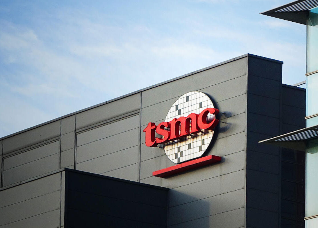
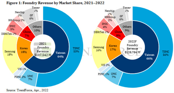
AMD Said to Become TSMC's Third Largest Customer in 2023
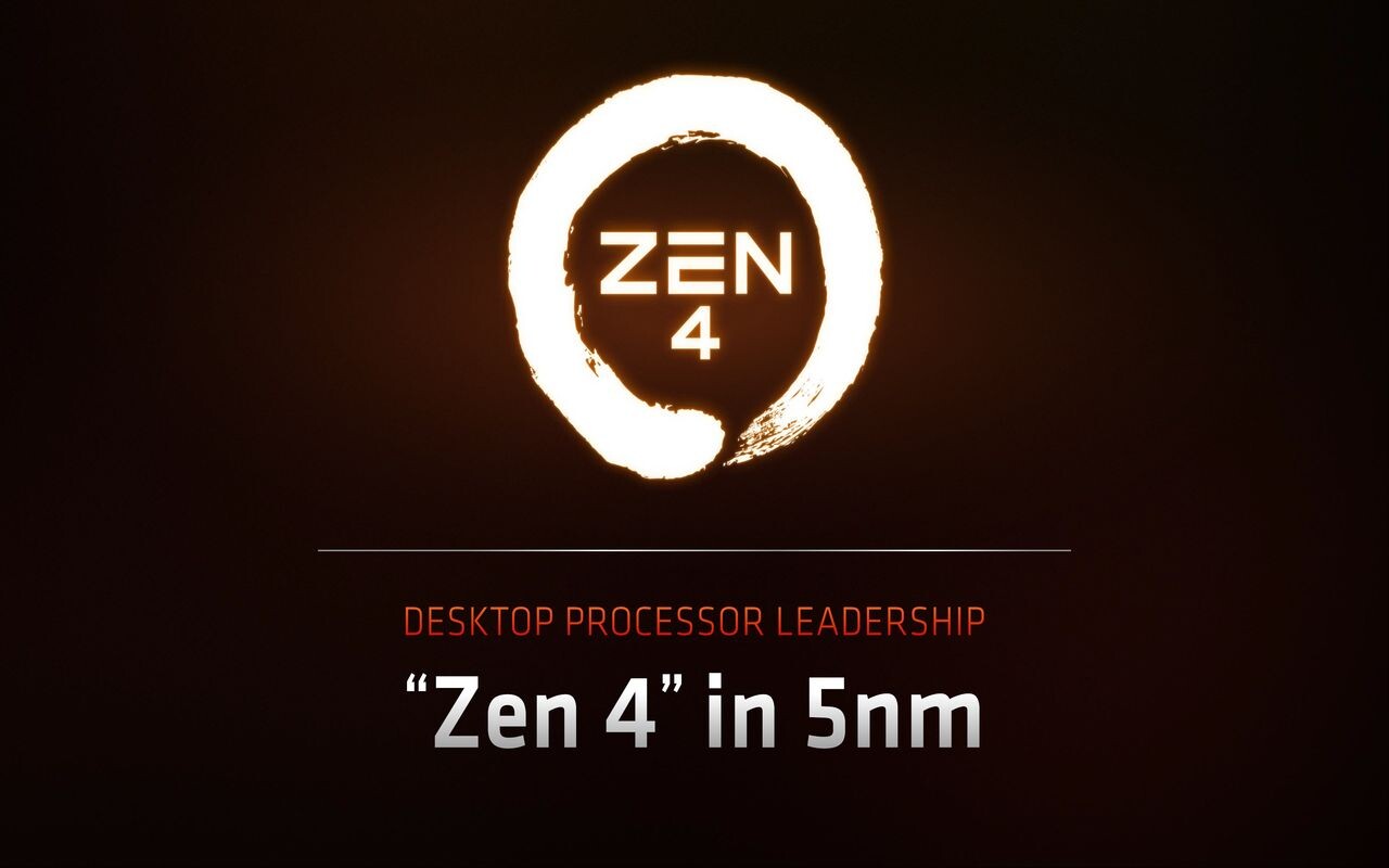
Based on a report in the Taiwanese media, AMD is quickly becoming a key customer for TSMC and is expected to become its third largest customer in 2023. This is partially due to new orders that AMD has placed with TSMC for its 5 nm node. AMD is said to become TSMC's single largest customer for its 5 nm node in 2023, although it's not clear from the report how large of a share of the 5 nm node AMD will have.
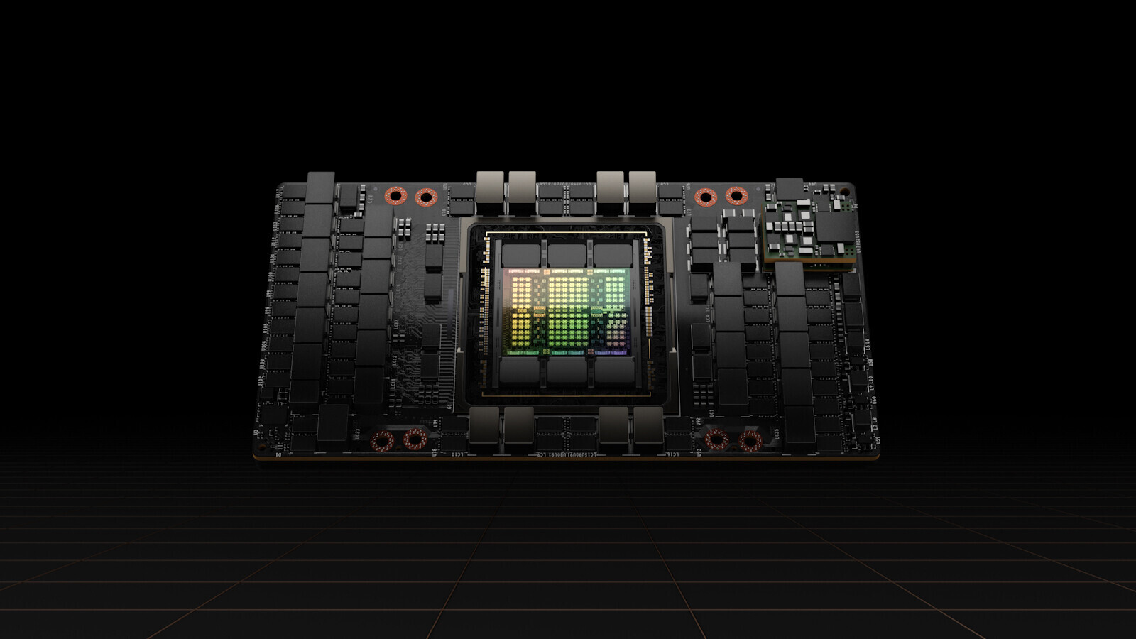
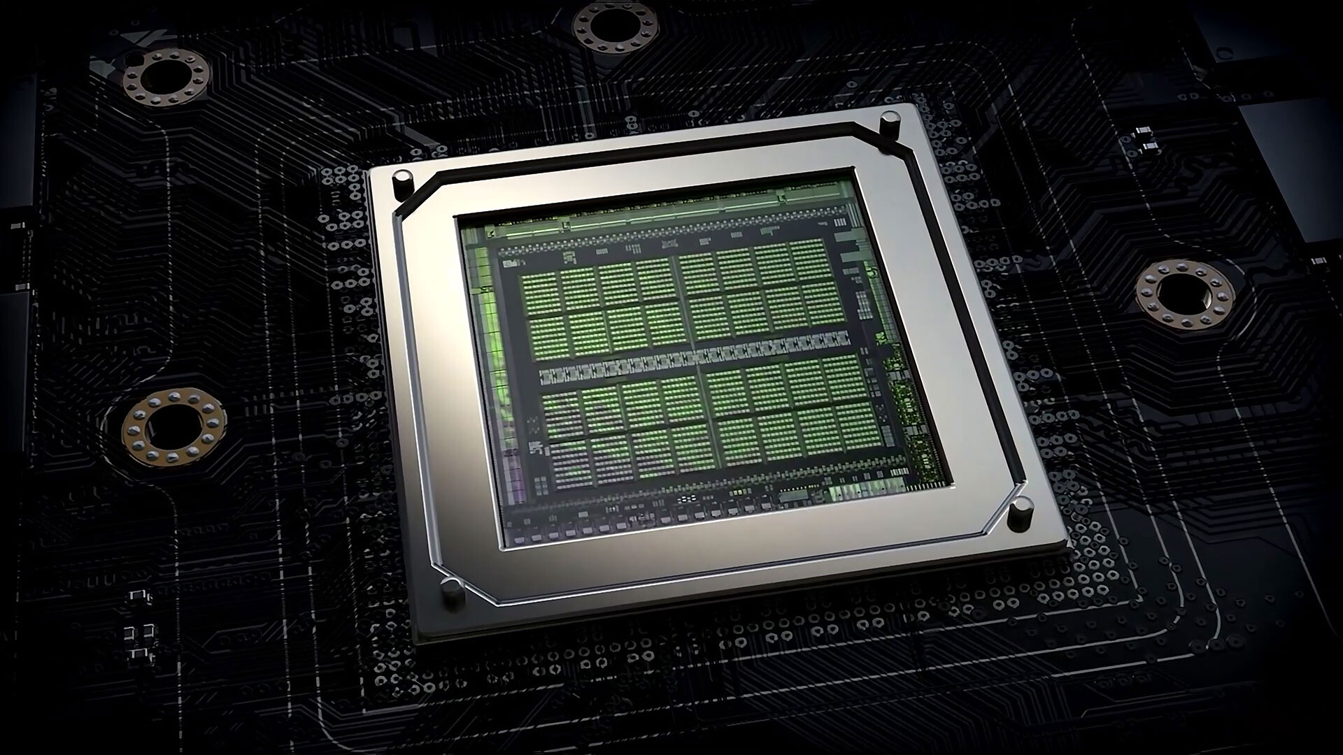
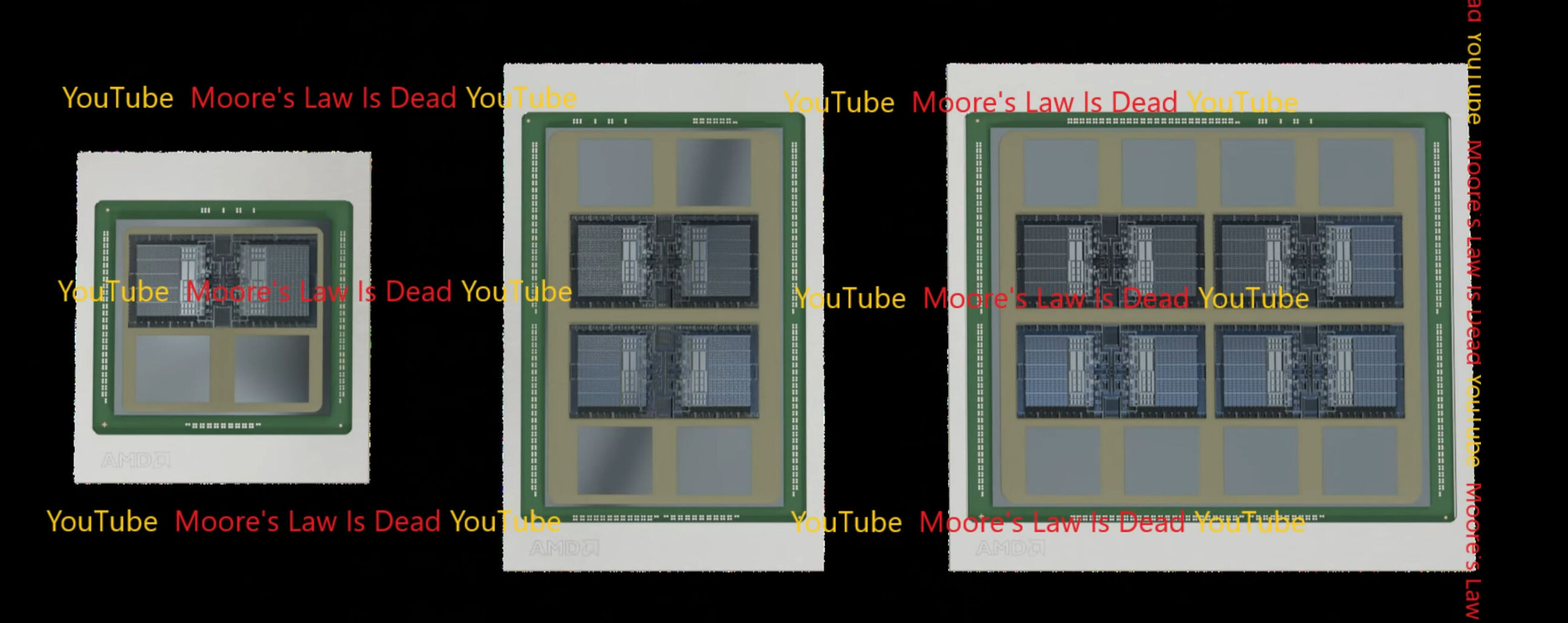
The additional orders are said to be related to AMD's Zen 4 based processors, as well as its upcoming RDNA3 based GPUs. AMD is expected to be reaching a production volume of some 20,000 wafers in the fourth quarter of 2022, although there's no mention of what's expected in 2023. Considering most of AMD's products for the next year or two will all be based on TSMC's 5 nm node, this shouldn't come as a huge surprise though, as AMD has a wide range of new CPU and GPU products coming.
The additional orders are said to be related to AMD's Zen 4 based processors, as well as its upcoming RDNA3 based GPUs. AMD is expected to be reaching a production volume of some 20,000 wafers in the fourth quarter of 2022, although there's no mention of what's expected in 2023. Considering most of AMD's products for the next year or two will all be based on TSMC's 5 nm node, this shouldn't come as a huge surprise though, as AMD has a wide range of new CPU and GPU products coming.