News Posts matching #Tahiti

Return to Keyword Browsing

AMD Teases Polaris 10 and Polaris 11 ASIC Images

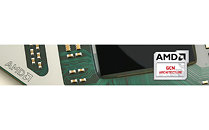
AMD posted a new webpage for its upcoming "Polaris" GPU architecture, outlining its various innovations - 4th gen. Graphics CoreNext, 4K H.265 60 Hz game-streaming, next-generation display engine with support for DisplayPort 1.3 and HDMI 2.0, XConnect Technology, and the foundation of GPUOpen. In this page, the company inadvertently leaked pictures of its upcoming Polaris 10 "Ellesmere" and Polaris 11 "Baffin" ASICs.

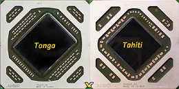
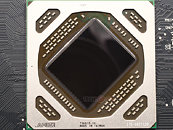
The mast image of the page has a faded 3-quarter shot of a "small" GPU with a die that's almost 30% of the package area. This hints at Polaris 11 "Baffin." This chip is rumored to feature a 128-bit GDDR5/GDDR5X memory interface, and so its pin-count, and conversely, package-size is less. Then in its "4th gen GCN" heading image, AMD showed a picture of a bigger GPU. At first glance, you could assume that it's either "Tonga XT" or "Tahiti" looking at its support brace, but VideoCardz observed that the on-package electrical components in this image are arranged nothing like on the "Tonga" or "Tahiti." This could very well be Polaris 10 "Ellesmere."

AMD "Fiji" GPU Die-shot Revealed by Chipworks

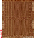
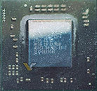
VLSI technical publication Chipworks posted the first clear die-shot of AMD's "Fiji" silicon, revealing intricate details of the most technically advanced GPU. What makes Fiji the most advanced graphics chip is its silicon interposer and stacked HBM chips making up a multi-chip module. It's the die in the center of all that, which went under Chipworks' microscope.

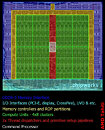
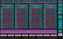
The die-shot reveals a component layout that's more or less an upscale of "Tonga." Some of the components, such as the front-end appear to be entirely identical to "Tahiti" or "Tonga." The shot reveals the 64 GCN compute units arranged in four rows, on either side of the central portion with the dispatch and primitive setup pipelines. The pad-area of the on-die memory controllers appear to be less than the large memory I/O pads that made up the 384-bit interface of "Tahiti." The first picture below is the die-shot of "Fiji," followed by a color-coded die-shot of "Tahiti."
AMD Radeon Graphics Roadmap for 2015 Leaked

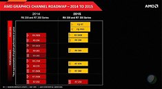
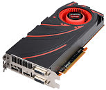
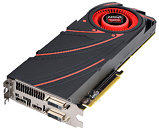
It looks like AMD's desktop discrete GPU lineup for 2015 will see a mix of rebrands, re-codename, and one big new chip, all making up the new Radeon R7 300 and R9 300 series. Cards based in this lineup should begin rolling out this month. Leaks from OEMs such as this one, suggest that the first of these should begin rolling out as early as June 16.

The spread is pretty cut and dry. "Hawaii," the chip driving the R9 290 series, will not only get a new codename as "Grenada," but also a seamless rebrand to the R9 390 series, with Grenada Pro making up the R9 390, and Grenada XT making up the R9 390X. One possibility could be AMD taking advantage of low 4 Gbit GDDR5 chip prices to cram 8 GB of standard memory amount, across Grenada's 512-bit wide memory interface. The R9 390X will compete with the GeForce GTX 970, while the R9 390 will offer an option in the vast price and performance gorge between the GTX 960 and GTX 970.

AMD Radeon R9 380 Launched by PC OEM

Earlier this day, HP announced its newest line of desktop PCs, one of which comes with a curious-sounding Radeon R9 380 graphics card. HP's product pages for its new desktops aren't active, yet, leaving us to only speculate on what the R9 380 could be. One theory making rounds says that the R9 380 could either be a re-branded R9 285, or be based on its "Tonga" silicon, which physically features 2,048 stream processors based on Graphics CoreNext (GCN) 1.2 architecture, and a 384-bit wide GDDR5 memory interface. Another theory states that the R9 380 could be an OEM-only re-brand of the R9 280 or R9 280X, based on the 3+ year old "Tahiti" silicon.

The former theory sounds more plausible, because re-branding a "Tahiti" based product would be suicidal for AMD. Although based on GCN, "Tahiti" lacks a lot of architecture features introduced with "Hawaii" and "Tonga." AMD practically stopped optimizing games for "Tahiti," and some of its new features, such as FreeSync and XDMA CrossFire, can't be implemented on it. "Tonga," on the other hand, supports both these features, and one can create an SKU with all its 2,048 stream processors, and its full 384-bit GDDR5 memory interface unlocked. If the R9 380 is indeed an OEM-only product, then it's likely that the company's retail-channel products could be branded in the succeeding R9 400 series. GPU makers tend to re-brand and bump their SKUs by a series for OEMs to peddle in their "new" products at short notice.

AMD "Tonga" Silicon Features 384-bit Wide Memory Interface

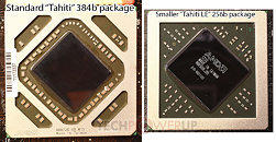
In what could explain the rather large die-size and transistor-count of AMD's "Tonga" silicon, compared to "Tahiti," it turns out that the silicon features a 384-bit wide GDDR5 memory interface, and not the previously thought of 256-bit wide one. The die is placed on a package with pins for just 256-bit, on the Radeon R9 285, but it can be placed on a bigger package, with more pins, to wire out the full width of the memory bus, in future SKUs. This isn't the first time AMD has done something like this. Its "Tahiti LE" chip was essentially a "Tahiti" die placed on a smaller package with pins for just a 256-bit wide memory bus, on the oddball Radeon HD 7870 XT.

What this means is that AMD's next performance-segment graphics card based on the "Tonga" silicon, could feature 50% more memory bandwidth than the R9 285. The stream processor count is still 2,048, but these are more advanced Graphics CoreNext 1.2 stream processors, compared to first-generation ones on "Tahiti," offering more performance per Watt. The TMU count remains 128, although there's no clarity on the ROP count. Estimates are split between 32 and 48. The R9 285 has 32, and so does "Tahiti."

AMD Radeon R9 285 Launch Date Revealed

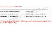
AMD is set to launch its new performance-segment graphics card, the Radeon R9 285, on the 2nd September, 2014. Ahead of its launch, the company is expected to tease the card at its August 23rd press-event, celebrating 30 years of graphics and gaming. On that day, AMD will share "partial" details of the card.

The R9 285 is based on AMD's swanky new 28 nm "Tonga" silicon, which is being drummed up to be AMD's best answer to NVIDIA's GK104. The chip offers performance rivaling "Tahiti," at the power consumption of GK104. The R9 285 is being designed to offer performance roughly that of the Radeon R9 280, at energy-efficiency, and pricing to drop lead on NVIDIA's GeForce GTX 760. A month later, presumably in early October, the company plans to launch the faster R9 285X, offering performance comparable (if not higher than) the R9 280X, at the energy-efficiency levels of GTX 770. "Tonga" physically features 2,048 Graphics CoreNext 1.1 stream processors, 128 TMUs, 32 ROPs, and a 256-bit wide GDDR5 memory interface, which will hold 2 GB or 4 GB of memory.

Sapphire Radeon R9 285 "Tonga" Pictured

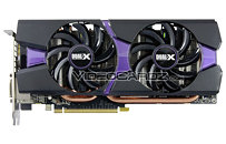
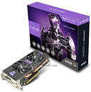
Here are the first pictures of the card AMD hopes to take on NVIDIA's bestselling GeForce GTX 760 with, the Radeon R9 285. This particular one, branded by Sapphire, featuring its Dual-X cooling solution. The R9 285 is based on a brand new chip by AMD, codenamed "Tonga." It's rumored to feature the same stream processor count as one of the "Tahiti" variants, while featuring higher clocks, and a narrower 256-bit wide GDDR5 memory interface, a fact confirmed by this card's marketed 2 GB of memory. Given how marketing material of the R9 285 is ready, its launch may not be far away.

AMD "Tonga" GPU Arrives This August

In a bid to counter NVIDIA's bestselling GeForce GTX 760, AMD is preparing a new 28 nm GPU, codenamed "Tonga," as detailed in our older article on the chip. At the time of its writing, we had two theories on what "Tonga" could be, one held that it could be a counter to the GM107, and the other, that's is a step above "Curacao," in a bid to counter the GTX 760. We're now learning that AMD could launch the first graphics cards based on this chip, some time in August. The chip will replace the ailing "Tahiti Pro" silicon, from which is carved out the Radeon R9 280. While the R9 280 offers performance competitive to the GTX 760, it loses out big time on power consumption and heat. The cheaper R9 270X, on the other hand, offers lower performance, and similar power levels. "Tonga" could offer nearly as much performance, while featuring a new combination of components, that help AMD lower not just power draw, but also overall costs.

The 28 nm "Tonga" silicon is expected to feature 2,048 GCN2 stream processors, 128 TMUs, 32 ROPs, and a 256-bit wide GDDR5 memory interface. You'll notice that its memory interface is narrower than that of the R9 280, but performance is made up for with a higher stream processor count, and probably higher clock speeds, too. The card could come in memory capacities of 2 GB, with some manufacturers innovating 4 GB variants. There's no word on what the company could end up naming the first cards running this chip.

MSI Announces Radeon R9 280 Gaming

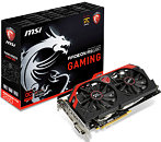
MSI finally launched its first Radeon R9 280 graphics card, flashing its Gaming Series branding. Based on an otherwise identical board design to that of the R9 280X Gaming, the card features MSI's Twin Frozr IV cooling solution. It offers factory-overclocked speeds of 933 MHz core, 1000 MHz boost, and 5.00 GHz memory. Based on the 28 nm "Tahiti" silicon, the Radeon R9 280 offers 1,792 stream processors, 112 TMUs, 32 ROPs, and a 384-bit wide GDDR5 memory interface, holding 3 GB of memory. The card draws power from a combination of 6-pin and 8-pin PCIe power connectors, display outputs include two mini-DisplayPort connectors, two dual-link DVI, and an HDMI connector. Expect this one to go for around $280.

AMD Chases Crucial $279 Price Point with Radeon R9 280

AMD's Radeon R9 200 series appears to have come a full circle with the company launching the Radeon R9 280, to capture the crucial US $279.99 price point, going against NVIDIA's GeForce GTX 760. The R9 280 isn't too different from the Radeon HD 7950 from the previous generation, featuring higher clock speeds, and PowerTune with boost. Based on the 28 nm "Tahiti" silicon, the R9 280 features 1,792 Graphics CoreNext stream processors, 112 TMUs, 32 ROPs, and a 384-bit wide GDDR5 memory interface, holding 3 GB of memory. The card features clock speeds of 827 MHz core, 933 MHz boost, and 5.00 GHz memory. The R9 280 is rated with the same 250W average board power as the R9 280X. AMD add-in board (AIB) partners have launched custom-design boards, including ones that feature factory overclocked speeds.

AMD to Release Radeon R9 280X Revision this Late-November

AMD is planning to release a revision of the Radeon R9 280X this late-November, based on the new "Tahiti-XTL" silicon. Originally designed to be based on that ASIC, the R9 280X ended up being based on "Tahiti XT2," the same exact ASIC that drives the Radeon HD 7970 GHz Edition, as "Tahiti XTL" wasn't ready for its early-October launch. The new silicon promises lower power consumption, heat output, and in turn, lower fan noise output. AMD won't announce the revision, but perform a "running change" for its add-in board partners. The only way you'll be able to tell it's a "Tahiti XTL" based R9 280X, apart from disassembling the card, will be reading its BIOS.

AMD "Hawaii" Architecture Diagram Leaked

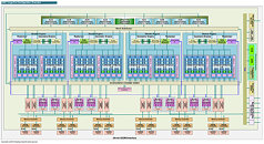
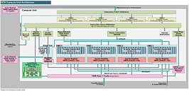
An alleged company slide detailing the architecture of AMD's upcoming "Hawaii" GPU was leaked to the web, revealing a monstrous combination of components. The GPU maintains the same component hierarchy as "Tahiti." The most distinguishing feature here is that whereas "Tahiti" features two shader engines, "Hawaii" features four. What it translates to, is double the geometry processing power, four independent geometry processors with a tessellation unit each, and double the number of ROPs, at 64. Each shader unit features 11 compute units (CU), the number-crunching machinery of the GPU. Each CU holds 4 TMUs (texture memory units), and 64 stream processors.

The four shader engines of "Hawaii" are tied to a unified command processing structure, a 1 megabyte L2 cache, a 512-bit wide GDDR5 memory interfaces, and the ancillaries, that include the PCI-Express 3.0 x16 bus interface, six display controllers (six TMDS links in all), CrossFireX XDMA, and multimedia accelerators that include UVD (accelerates high-def video), VCE (video codec engine, accelerates multimedia codecs), and the new TrueAudio hardware DSP.

Radeon R9 280X CrossFire-compatible with Radeon HD 7900 Series

AMD offers greater flexibility with its multi-GPU solutions, letting you mix and match any two GPUs based on the same silicon. It was quite natural to expect a Radeon R9 280X to work in tandem with a Radeon HD 7970 GHz Edition from the previous generation, since the two are based on the same "Tahiti" GPU, which is now proven. HardwareCanucks managed to run that combo without a hitch, and log performance results across a bouquet of game tests. The publication also notes that one should be able to similarly pair a Radeon R9 270X with a Radeon HD 7870 GHz Edition (the one based on "Pitcairn," not "Tahiti LE"). Have a Radeon HD 7950? Feel free to add an R9 280X to the mix.

Radeon R9 290X Features 64 ROPs

A leaked company slide by AMD confirmed that its high-end "Hawaii" silicon indeed features 64 raster operations units (ROPs). In reference to its predecessor, "Tahiti," the slide speaks of 2 times the ROPs (32 on "Tahiti") and 1.4 times the stream processors (2048 on "Tahiti," so 2816 on "Hawaii"). Other known specifications include up to 1 GHz GPU clock, up to 5.00 GHz memory clock, and a 512-bit wide GDDR5 memory interface, holding 4 GB of memory. Reviews of Radeon R9 290X could surface around mid-October.

AMD Announces Market Availability of Radeon R9 and R7 Series

AMD announced market availability of several of its new Radeon R9 and Radeon R7 series discrete graphics SKUs. Leading the pack for today's launch is the Radeon R9 280X. Heavily based on the Radeon HD 7970 GHz Edition, the card is priced at $299, and is designed to offer an interesting price-performance combination. In raw performance, it competes with the now $410 GeForce GTX 770, yet it's priced just $50 more than the $249 GeForce GTX 760. Based on the same 28 nm "Tahiti" silicon as the HD 7970 GHz Edition, it features clock speeds of 1000 MHz core, with 6.00 GHz memory. It features 2,048 stream processors, 128 TMUs, 32 ROPs, and a 384-bit wide GDDR5 memory interface, holding 3 GB of memory.

The next card on AMD's block is the Radeon R9 270X, which is designed to strike a price-performance sweet-spot at $199. Essentially an overclocked Radeon HD 7870 GHz Edition, the card is based on the 28 nm "Pitcairn" silicon, featuring clock speeds of 1050 MHz core, and 6.40 GHz memory. It features 1,280 stream processors, 80 TMUs, 32 ROPs, and a 256-bit wide GDDR5 memory interface, holding 2 GB of memory. Lastly, there's the Radeon R7 260X, an interesting sub-$150 product, priced at $139. Based on the same "Bonaire" silicon as the Radeon HD 7790, it features higher clock speeds, and double the standard memory amount. It features clock speeds of 1100 MHz, and 6.50 GHz memory. The chip features 896 stream processors, 56 TMUs, 16 ROPs, and a 128-bit wide GDDR5 memory interface, holding 2 GB of memory. The three cards will launch through the various AMD add-in board (AIB) partners, in their non-reference designs.

Radeon R9 270X a Faster Radeon HD 7870 "Tahiti LE"

AMD's performance-segment Radeon R9 270X could prove to be a winning sub-$200 product for the company. Sources affiliated with a leading online retailer revealed that the SKU could greatly resemble the limited edition Radeon HD 7870 "Tahiti LE," possibly with higher clock speeds and stream processor count. "Tahiti LE" is a major variation of "Tahiti," which features not just lower numbers of stream processors and TMUs, but also a narrower 256-bit wide GDDR5 memory interface. The die is mated with a more compact BGA package that has lower pin count, thanks to the narrower memory interface, and probably fewer power/ancillary connections. Sources reveal the R9 270X to be "a crippled HD 7950," which could indicate a stream processor count of 1792, higher than the 1536 of Radeon HD 7870 "Tahiti LE." The TMU count could be proportionately higher due to the way they're structured on the GPU; at 112, compared to 96 on "Tahiti LE." The clock speeds are still under the wraps. AMD set an SEP price of the Radeon R9 270X at $199.

XFX Radeon R9 280X Double Dissipation Pictured

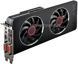
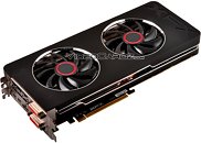
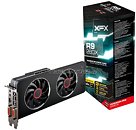
Although Radeon R9 280X has a lot in common with Radeon HD 7970 GHz Edition, AMD's AIB partners are expected to come up with entirely new board designs. A case in point is the XFX Double Dissipation card, pictured below. While we don't know if XFX is recycling PCB designs over from the HD 7970 GHz Edition, the cooler certainly looks new, with its tall and chunky aluminium fin heatsink that's fed by copper heat-pipes, and a pair of 100 mm fans. Its box speaks of an "unlocked voltage" feature.

Based on the 28 nm "Tahiti XTL" silicon, Radeon R9 280X features 2,048 GCN stream processors, 128 TMUs, 32 ROPs, and a 384-bit wide GDDR5 memory interface, holding 3 GB of memory. The GPU is expected to be clocked a notch above 1.00 GHz on XFX' card, and the memory around 6.40 GHz. Slated for October 3rd, the card is expected to be priced anywhere between $299 and $329.

Radeon R9 and Radeon R7 Graphics Cards Pictured Some More

Here's a quick recap of AMD's updated product stack, spread between the R9 and R7 series. This article can help you understand the new nomenclature. AMD's lineup begins with the Radeon R7 250 and Radeon R7 260X. The two are based on the 28 nm "Curacao" silicon, which is a variation of the "Pitcairn" silicon the previous-generation Radeon HD 7870 was based on. The R7 250 is expected to be priced around US $89, with 1 GB of RAM, and performance rated at over 2,000 points by 3DMark Firestrike benchmark. The R7 260X, features double the memory at 2 GB, higher clock speeds, possibly more number crunching resources, Firestrike score of over 3,700 points, and a pricing that's around $139. This card should turn up the heat against the likes of GeForce GTX 650 Ti Boost.

Moving on, there's the $199 Radeon R9 270X. Based on a chip not much unlike "Tahiti LE," it features 2 GB of memory, and 3DMark Firestrike score of over 5,500 points. Then there's the Radeon R9 280X. This card, priced attractively at $299, is practically a rebrand of the Radeon HD 7970 GHz Edition with. It features 3 GB of RAM, and over 6,800 points on 3DMark Firestrike. Then there are the R9 290 and R9 290X. AMD flew dozens of scribes thousands of miles over to Hawaii, and left them without an official announcement on the specifications of the two. From what AMD told us, the two feature 4 GB of memory, over 5,000 TFLOP/s compute power, and over 300 GB/s memory bandwidth. The cards we mentioned are pictured in that order below.

More pictures follow.

HIS Puts Out Next Generation Radeon Family SKU Names

HIS posted placeholders on its website for various Radeon Rx 200 series products, before redacting it, but not before VideoCardz took a screengrab. The placeholders reveal nothing about the products, but their names, which include GPU name, memory (type/amount), and custom cooling solution, if any. The Radeon R9 280X IceQ X² leads the pack for HIS. There's nothing known just yet, but the listing reveals 3 GB of GDDR5 memory, and a custom cooling solution by HIS. From the R9 280X, HIS jumps straight down to the mainstream R7 250, and R7 240, with IceQ and iCooler variants of each, and variants based on slower DDR3 memory. The codename "Tahiti XTL" is floating around with the R9 280X. It could be anything from a cut-down 28 nm "Tahiti" silicon, to just a low-power variant of "Tahiti" as configured and clocked on the Radeon HD 7970 GHz Edition. The real stuff (new high-end GPUs), is reserved for the R9 290 series (if there is one).
A list of SKUs by HIS follows:

AMD "Hawaii" Press Sample Boxes Surface

Some time in late September, the 25th to be precise, AMD is flying the press at large over to Hawaii, to unveil its "Volcanic Islands" GPU family, with its flagship part, codenamed "Hawaii." This chip is expected to succeed "Tahiti," on which AMD's top-end Radeon HD 7900 series is based. An poster on ChipHell forums leaked these pictures of a press-package of AMD's flagship Hawaii-based graphics card, which has things going both for and against its credibility.

To begin with, the picture shows an audio CD-type jewel case holding Battlefield 4. Given that the game won't launch until late-October, we find it implausible that its release DVDs will be ready a month in advance. There's also a graphic printed on the box that shows the shore of a volcanic island (where magma meets the ocean) in the background, and an AMD logo in the foreground. The thread also contains a few alleged x-ray shots from a different poster, but we're pretty sure that they're of a motherboard. Nice try.

Sapphire Radeon HD 7990 Atomic PCB and Cooling Solution Pictured

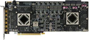
Sapphire's Radeon HD 7990 Atomic made its first appearance at Computex, early last month. While launch of the card itself is less than a few weeks away, pictures of its PCB and cooling solution made it to the web. Its PCB, pictured below, features a pair of 28 nm "Tahiti XT2" GPUs, a total of 6 GB of GDDR5 memory, and a PLX PEX8747 PCI-Express gen 3.0 x48 bridge chip, powered by a gargantuan 18-phase VRM that draws power from three 8-pin PCI-Express power connectors.

Each GPU system hence gets a 6+2+1 phase power supply (Vcc+VDDCI+MVDD). The Vcc phases appear to consist of two 50A chokes per phase, and driver-MOSFETs; while the ancillary phases use more conventional LFPAK MOSFETs. Tantalum capacitors handle most electricals on this 12-layer PCB. The PCB features two sets of video BIOS for each GPU. Display outputs include six mini-DisplayPort connectors. The card can pair with any other Radeon HD 7900 series card using CrossFireX.

Radeon HD 9000 Series Arrives This October: Report

When AMD re-branded most of its Radeon HD 7000 series SKUs to HD 8000 series, for OEMs, we saw this coming from a parsec away. AMD's next discrete GPU family for the retail channel will be placed along the Radeon HD 9000 series, and it debuts no later than this October, according to a Guru3D report. Interestingly, the report states that the first parts in the family will be based on existing 28 nanometer silicon fab processes, and will be codenamed "Curacao" and "Hainan."

We've had our run-ins with "Curacao," from time to time. It's been rumored to be an upgrade of existing "Tahiti" silicon, with 2,304 stream processors based on Graphics CoreNext 2.0 architecture, 144 TMUs, 48 ROPs, and a 384-bit wide GDDR5 memory interface. The Guru3D report adds to that with the mention of an improved front-end, which adds four asynchronous computing engines (ACEs), and three independent geometry engines.

GIGABYTE Joins the HD 7990 Party

Albeit a wee bit late, GIGABYTE joined the Radeon HD 7990 launch party with a card of its own (model: GV-R799D5-6GD-B). Pictured below, GIGABYTE's offering is no different from any of the HD 7990 cards launched this Wednesday, except the company decals on the card. It sticks to AMD reference clock speeds of 1000 MHz core, and 6.00 GHz memory, featuring 6 GB of it. The dual-GPU graphics card runs a pair of 28 nm "Tahiti" GPUs, each featuring 2048 stream processors, 128 TMUs, 32 ROPs, and 384-bit wide memory interfaces. The card draws power from two 8-pin PCIe power connectors, outputs include four mini-DisplayPort and a dual-link DVI. On par with every other card, GIGABYTE's HD 7990 will cost $999.

HIS Rolls Out its Radeon HD 7990 Graphics Card

HIS joined the Radeon HD 7990 "Malta" party by launching its own card, which predictably, is based on AMD's reference design. Called HIS HD 7990 Fan, the card features AMD-reference clock speeds of 1000 MHz core and 6.00 GHz memory; and features the "whisper quiet" triple-fan cooling solution. The card features a pair of 28 nm "Tahiti" GPUs, each featuring 2048 stream processors, 128 TMUs, 32 ROPs, and 384-bit wide GDDR5 memory interfaces. There is a total of 6 GB of memory on board. AMD's Never Settle Reloaded, with eight games, come included. The HIS HD 7990 Fan is expected to be priced at US $999.

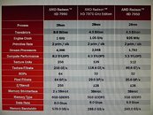
AMD Radeon HD 7990 Clock Speeds and Core Config Confirmed, Tested

Ahead of its April 24 launch, AMD board vendors has been distributing marketing materials to their retail partners. One such retailer in Japan revealed the flagship graphics card's specifications sheet, revealing details such as clock speeds and GPU core configuration.

To begin with, AMD isn't compromising much on clock speeds on the HD 7990 "Malta," in an effort to lower power draw. The card features GPU core clock speed of 1000 MHz, which puts it above the single-GPU Radeon HD 7970, but not much lower than the Radeon HD 7970 GHz Edition, with its 1050 MHz. The memory is clocked at 6.00 GHz, on par with the HD 7970 GHz Edition, which yields a cumulative memory bandwidth of 576 GB/s.
Return to Keyword Browsing
Nov 23rd, 2024 20:49 EST change timezone

New Forum Posts

Popular Reviews

Controversial News Posts