Samsung Electronics Announces First Quarter 2025 Results
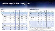
Samsung Electronics today reported financial results for the first quarter ended March 31, 2025. The Company posted KRW 79.14 trillion in consolidated revenue, an all-time quarterly high, on the back of strong sales of flagship Galaxy S25 smartphones and high-value-added products. Operating profit increased to KRW 6.7 trillion despite headwinds for the DS Division, which experienced a decrease in quarterly revenue.
The Company has allocated its highest-ever annual R&D expenditure for 2024, and in the first quarter of this year, it has also increased its R&D expenditure by 16% compared to the same period last year, amounting to 9 trillion won. Despite the growing macroeconomic uncertainties due to recent global trade tensions and slowing global economic growth, making it difficult to predict future performance, the Company will continue to make various efforts to secure growth. Additionally, assuming that the uncertainties are diminished, it expects its performance to improve in the second half of the year.
The Company has allocated its highest-ever annual R&D expenditure for 2024, and in the first quarter of this year, it has also increased its R&D expenditure by 16% compared to the same period last year, amounting to 9 trillion won. Despite the growing macroeconomic uncertainties due to recent global trade tensions and slowing global economic growth, making it difficult to predict future performance, the Company will continue to make various efforts to secure growth. Additionally, assuming that the uncertainties are diminished, it expects its performance to improve in the second half of the year.


