News Posts matching #accelerator

Return to Keyword Browsing

Micron HBM Designed into Leading AMD AI Platform

Micron Technology, Inc. today announced the integration of its HBM3E 36 GB 12-high offering into the upcoming AMD Instinct MI350 Series solutions. This collaboration highlights the critical role of power efficiency and performance in training large AI models, delivering high-throughput inference and handling complex HPC workloads such as data processing and computational modeling. Furthermore, it represents another significant milestone in HBM industry leadership for Micron, showcasing its robust execution and the value of its strong customer relationships.

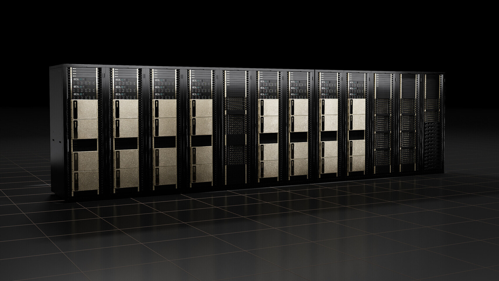
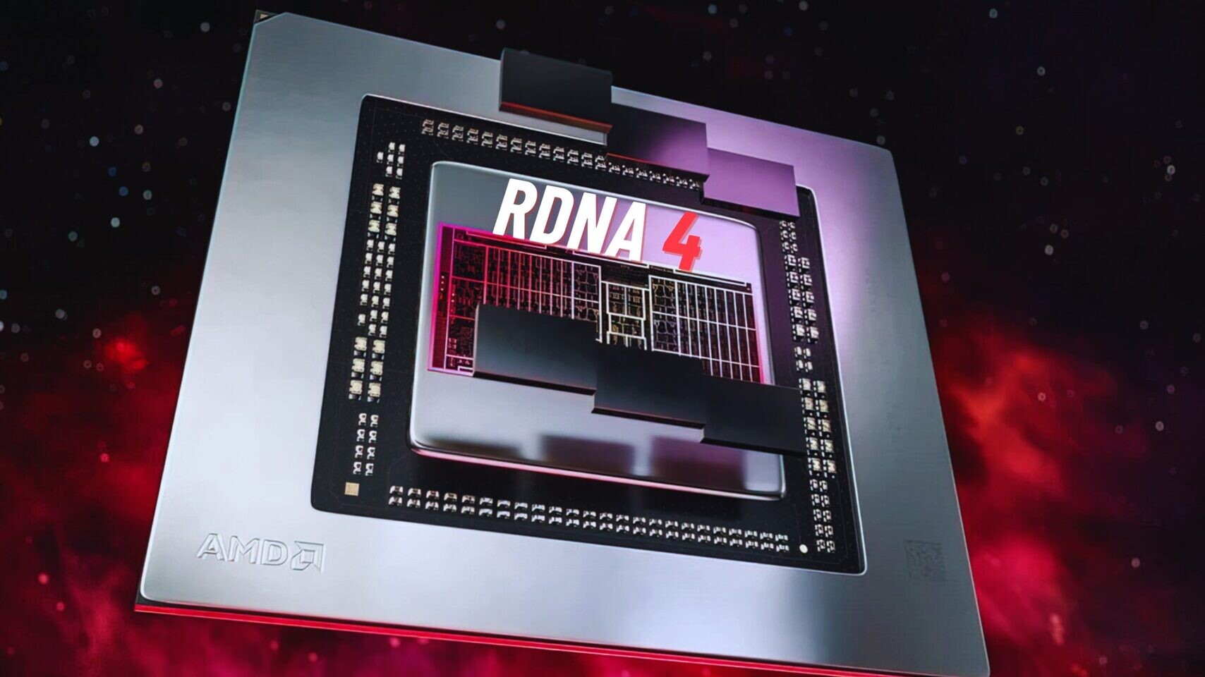
Micron HBM3E 36 GB 12-high solution brings industry-leading memory technology to AMD Instinct MI350 Series GPU platforms, providing outstanding bandwidth and lower power consumption. The AMD Instinct MI350 Series GPU platforms, built on AMD advanced CDNA 4 architecture, integrate 288 GB of high-bandwidth HBM3E memory capacity, delivering up to 8 TB/s bandwidth for exceptional throughput. This immense memory capacity allows Instinct MI350 series GPUs to efficiently support AI models with up to 520 billion parameters—on a single GPU. In a full platform configuration, Instinct MI350 Series GPUs offers up to 2.3 TB of HBM3E memory and achieves peak theoretical performance of up to 161 PFLOPS at FP4 precision, with leadership energy efficiency and scalability for high-density AI workloads. This tightly integrated architecture, combined with Micron's power-efficient HBM3E, enables exceptional throughput for large language model training, inference and scientific simulation tasks—empowering data centers to scale seamlessly while maximizing compute performance per watt. This joint effort between Micron and AMD has enabled faster time to market for AI solutions.

NVIDIA Reportedly Progressing Well with "Rubin" AI GPU Development - Insiders Foresee Q3'25 Sampling

Over a year ago, industry moles started chattering about a potential "late 2025" launch of NVIDIA "Rubin" AI accelerators/ GPUs. According to older rumors, one of the successors to current-gen "Blackwell" hardware could debut in chiplet-based "R100" form. Weeks ahead of Christmas 2024, Taiwanese insider reports pointed to Team Green's development of the "Rubin" AI project being sixth months ahead of schedule. Despite this extra positive outlook, experts surmised that the North American giant would not be rushing out shiny new options—especially with the recent arrival of "Blackwell Ultra" products. A lot of leaks seem to be coming from sources at (or adjacent to) TSMC.

Taiwan's top foundry service is reportedly in the "Rubin" equation; with a 3 nm (N3P) node process and CoWoS-L packaging linked to "R100." According to local murmurs, the final "taping out"—of Rubin GPUs and Vera CPUs—is due for completion this month. Trial production is expected run throughout the summer, with initial samples being ready for distribution by September. According to a fresh Ctee TW news report, unnamed supply chain participants reckon that NVIDIA's "new chip development schedule is smoother than before, and mass production (of Rubin and Vera chips) will begin as early as 2026." In theory, the first publicly exhibited final examples could turn up at CES 2026.

Chinese Tech Firms Reportedly Unimpressed with Overheating of Huawei AI Accelerator Samples

Mid-way through last month, Tencent's President—Martin Lau—confirmed that this company had stockpiled a huge quantity of NVIDIA H20 AI GPUs, prior to new trade restrictions coming into effect. According to earlier reports, China's largest tech firms have collectively spent $16 billion on hardware acquisitions in Q1'25. Team Green engineers are likely engaged in the creation of "nerfed" enterprise-grade chip designs—potentially ready for deployment later on in 2025. Huawei leadership is likely keen to take advantage of this situation, although it will be difficult to compete with the sheer volume of accumulated H20 units. The Shenzhen, Guangdong-based giant's Ascend AI accelerator family is considered to be a valid alternative to equivalent "sanction-conformant" NVIDIA products.

The controversial 910C model and a successor seem to be worthy candidates; as demonstrated by preliminary performance data, but fresh industry murmurs suggest teething problems. The Information has picked up inside track chatter from unnamed moles at ByteDance and Alibaba. During test runs, staffers noted the overheating of Huawei Ascend 910C trial samples. Additionally, they highlighted limitations within the Huawei Compute Architecture for Neural Networks (CANN) software platform. NVIDIA's extremely mature CUDA ecosystem holds a significant advantage here. Several of China's prime AI players—including DeepSeek—are reportedly pursuing in-house AI chip development projects; therefore positioning themselves as competing with Huawei, in a future scenario.

EdgeCortix SAKURA-II Enables GenAI on Raspberry Pi 5 and Arm Systems

EdgeCortix Inc., a leading fabless semiconductor company specializing in energy-efficient Artificial Intelligence (AI) processing at the edge, today announced that its industry leading AI accelerator, SAKURA-II M.2 Module is now available with Arm-based platforms, including Raspberry Pi 5 and AETINA's Rockchip (RK3588) platform, delivering unprecedented performance and efficiency for edge AI computing applications.

This powerful integration marks a major leap in democratizing real-time Generative AI capabilities at the edge. Designed with a focus on low power consumption and high AI throughput, the EdgeCortix SAKURA-II M.2 module enables developers to run advanced deep learning models directly on compact, affordable platforms like the Raspberry Pi 5—without relying on cloud infrastructure.

Xsight Labs Announced Availability of Its Arm-Based E1-SoC for Cloud and Edge AI Data Centers

Xsight Labs, a leading fabless semiconductor company providing end-to-end connectivity for next-generation hyperscale, edge and AI data center networks, today announced availability of its Arm -based E1-SoC for cloud and edge AI data centers. The E-Series is the only product of its kind to provide full control plane and data path programmability and is the industry's highest performance software-defined DPU (Data Processing Unit). Xsight Labs is taking orders now for its E1-SoC and the E1-Server, the first-to-market 800G DPU.

E1 is the first SoC in the E-Series, Xsight Labs' SDN (Software Defined Network) Infrastructure Processor product family of fully programmable network accelerators. Built on TSMC's advanced 5 nm process technology, the E1-SoC will begin shipping to customers and ecosystem partners.

Red Hat & AMD Strengthen Strategic Collaboration - Leading to More Efficient GenAI

Red Hat, the world's leading provider of open source solutions, and AMD today announced a strategic collaboration to propel AI capabilities and optimize virtualized infrastructure. With this deepened alliance, Red Hat and AMD will expand customer choice across the hybrid cloud, from deploying optimized, efficient AI models to more cost-effectively modernizing traditional virtual machines (VMs). As workload demand and diversity continue to rise with the introduction of AI, organizations must have the capacity and resources to meet these escalating requirements. The average datacenter, however, is dedicated primarily to traditional IT systems, leaving little room to support intensive workloads such as AI. To answer this need, Red Hat and AMD are bringing together the power of Red Hat's industry-leading open source solutions with the comprehensive portfolio of AMD high-performance computing architectures.

AMD and Red Hat: Driving to more efficient generative AI
Red Hat and AMD are combining the power of Red Hat AI with the AMD portfolio of x86-based processors and GPU architectures to support optimized, cost-efficient and production-ready environments for AI-enabled workloads. AMD Instinct GPUs are now fully enabled on Red Hat OpenShift AI, empowering customers with the high-performing processing power necessary for AI deployments across the hybrid cloud without extreme resource requirements. In addition, using AMD Instinct MI300X GPUs with Red Hat Enterprise Linux AI, Red Hat and AMD conducted testing on Microsoft Azure ND MI300X v5 to successfully demonstrate AI inferencing for scaling small language models (SLMs) as well as large language models (LLM) deployed across multiple GPUs on a single VM, reducing the need to deploy across multiple VMs and reducing performance costs.

AMD Prepares Instinct MI450X IF128 Rack‑Scale System with 128 GPUs

According to SemiAnalysis, AMD has planned its first-ever rack-scale GPU cluster for the second half of 2026, when it shows its first rack‑scale accelerator, the Instinct MI450X IF128. Built on what's expected to be a 3 nm‑class TSMC process and packaged with CoWoS‑L, each MI450X IF128 card will include at least 288 GB of HBM4 memory. That memory will sustain up to 18 TB/s of bandwidth, driving around 50 PetaFLOPS of FP4 compute while drawing between 1.6 and 2.0 kW of power. In our recent article, we outlined that AMD split the Instinct MI400 series into HPC-first MI430X and MI450X for AI. Now for AI-focused MI450X, the company created both an "IF64" backplane for simpler single‑rack installs and the full‑blown "IF128" for maximum density. The IF128 version links 128 GPUs over an Ethernet‑based Infinity Fabric network and uses UALink instead of PCIe to connect each GPU to three built‑in Pensando 800 GbE NICs. That design delivers about 1.8 TB/s of unidirectional bandwidth per GPU and a total of 2,304 TB/s across the rack.

With 128 GPUs each offering 50 PetaFLOPS of FP4 compute and 288 GB of HBM4 memory, the MI450X IF128 system delivers a combined 6,400 PetaFLOPS and 36.9 TB of high‑bandwidth memory, and MI450X IF64 provides about half of that. Since AI deployments require massive density of rack systems, AMD plans to possibly outnumber NVIDIA's upcoming system known as "Vera Rubin" VR200 NVL144 (144 compute dies, 72 GPUs), which tops out at 3,600 PetaFLOPS and 936 TB/s of memory bandwidth—about half of what AMD's IF128 approach promises. AMD will have a possibly more powerful system architecture than NVIDIA until the launch of VR300 "Ultra" NVL576, which has 144 GPUs, each carrying four compute dies, totaling 576 compute chiplets.

Report: Customers Show Little Interest in AMD Instinct MI325X Accelerators

AMD's Instinct MI325X accelerator has struggled to gain traction with large customers, according to extensive data from SemiAnalysis. Launched in Q2 2025, the MI325X arrived roughly nine months after NVIDIA's H200 and concurrently with NVIDIA's "Blackwell" mass-production roll-out. That timing proved unfavourable, as many buyers opted instead for Blackwell's superior cost-per-performance ratio. Early interest from Microsoft in 2024 failed to translate into repeat orders. After the initial test purchases, Microsoft did not place any further commitments. In response, AMD reduced its margin expectations in an effort to attract other major clients. Oracle and a handful of additional hyperscalers have since expressed renewed interest, but these purchases remain modest compared with NVIDIA's volume.

A fundamental limitation of the MI325X is its eight-GPU scale-up capacity. By contrast, NVIDIA's rack-scale GB200 NVL72 supports up to 72 GPUs in a single cluster. For large-scale AI inference and frontier-level reasoning workloads, that difference is decisive. AMD positioned the MI325X against NVIDIA's air-cooled HGX B200 NVL8 and HGX B300 NVL16 modules. Even in that non-rack-scale segment, NVIDIA maintains an advantage in both raw performance and total-cost-of-ownership efficiency. Nonetheless, there remains potential for the MI325X in smaller-scale deployments that do not require extensive GPU clusters. Smaller model inference should be sufficient for eight GPU clusters, where lots of memory bandwidth and capacity are the primary needs. AMD continues to improve its software ecosystem and maintain competitive pricing, so AI labs developing mid-sized AI models may find the MI325X appealing.

IBM Intros LinuxONE Emperor 5 Mainframe with Telum II Processor

IBM has introduced the LinuxONE Emperor 5, its newest Linux computing platform that runs on the Telum II processor with built-in AI acceleration features. This launch aims to tackle three key issues for tech leaders: better security measures, reduced costs, and smooth AI incorporation into business systems. The heart of the system, the Telum II processor, includes a second-generation on-chip AI accelerator. This component is designed to boost predictive AI abilities and large language models for instant transaction handling. The upcoming IBM Spyre Accelerator (set to arrive in late 2025) via PCIe card will boost generative AI functions. The platform comes with an updated AI Toolkit fine-tuned for the Telum II processor. It also offers early looks at Red Hat OpenShift AI and Virtualization allowing unified control of both standard virtual machines and containerized workloads.

The platform provides wide-ranging security measures. These include confidential computing strong cryptographic abilities, and NIST-approved post-quantum algorithms. These safeguard sensitive AI models and data from current risks and expected post-quantum attacks. When it comes to productivity, companies can combine several server workloads on one high-capacity system. This might cut ownership expenses by up to 44% compared to x86 options over five years. At the same time, it keeps exceptional 99.999999% uptime rates according to IBM. The LinuxOne Emperor 5 will run Linux Red Hat Enterprise Linux (RHEL), SUSE Linux Enterprise Server (SLES) and Canonical Ubuntu Server. Tina Tarquinio, chief product officer at IBM Z and LinuxONE, said: "IBM LinuxONE 5 represents the next evolution of our Linux infrastructure strategy. It is designed to help clients unlock the full potential of Linux and AI while optimizing their datacenters, simplifying their operations, and addressing risk. Whether you're building intelligent applications, deploying regulated workloads, consolidating infrastructure, or preparing for the next wave of transformation, IBM LinuxONE offers an exciting path forward."

Astera Labs Ramps Production of PCIe 6 Connectivity Portfolio

Astera Labs, Inc., a global leader in semiconductor-based connectivity solutions for AI and cloud infrastructure, today announced its purpose-built PCIe 6 connectivity portfolio is ramping production to fast-track deployments of modern AI platforms at scale. Now featuring gearbox connectivity solutions alongside fabric switches, retimers, and active cable modules, Astera Labs' expanding PCIe 6 portfolio provides a comprehensive connectivity platform to deliver unparalleled performance, utilization, and scalability for next-generation AI and general-compute systems. Along with Astera Labs' demonstrated PCIe 6 connectivity over optical media, the portfolio will provide even greater AI rack-scale distance optionality. The transition to PCIe 6 is fueled by the insatiable demand for higher compute, memory, networking, and storage data throughput, ensuring advanced AI accelerators and GPUs operate at peak efficiency.

Thad Omura, Chief Business Officer, said, "Our PCIe 6 solutions have successfully completed qualification with leading AI and cloud server customers, and we are ramping up to volume production in parallel with their next generation AI platform rollouts. By continuing to expand our industry-leading PCIe connectivity portfolio with additional innovative solutions that includes Scorpio Fabric Switches, Aries Retimers, Gearboxes, Smart Cable Modules, and PCIe over optics technology, we are providing our hyperscaler and data center partners all the necessary tools to accelerate the development and deployment of leading-edge AI platforms."

IBM Cloud is First Service Provider to Deploy Intel Gaudi 3

IBM is the first cloud service provider to make Intel Gaudi 3 AI accelerators available to customers, a move designed to make powerful artificial intelligence capabilities more accessible and to directly address the high cost of specialized AI hardware. For Intel, the rollout on IBM Cloud marks the first major commercial deployment of Gaudi 3, bringing choice to the market. By leveraging Intel Gaudi 3 on IBM Cloud, the two companies aim to help clients cost-effectively test, innovate and deploy GenAI solutions.

According to a recent forecast by research firm Gartner, worldwide generative AI (GenAI) spending is expected to total $644 billion in 2025, an increase of 76.4% from 2024. The research found "GenAI will have a transformative impact across all aspects of IT spending markets, suggesting a future where AI technologies become increasingly integral to business operations and consumer products."

VSORA Raises $46 Million to Produce its Jotunn8 AI Chip in 2025

SORA, a French innovator and the only European provider of ultra-high-performance artificial intelligence (AI) inference chips, today announced that it has successfully raised $46 million in a new fundraising round.

The investment was led by Otium and a French family office with additional participation from Omnes Capital, Adélie Capital and co-financing from the European Innovation Council (EIC) Fund.

Marvell Announces Successful Interoperability of Structera CXL Portfolio with AMD EPYC CPU and 5th Gen Intel Xeon Scalable Platforms

Marvell Technology, Inc., a leader in data infrastructure semiconductor solutions, today announced the successful interoperability of the Marvell Structera portfolio of Compute Express Link (CXL) with AMD EPYC CPUs and 5th Gen Intel Xeon platforms. This achievement underscores the commitment of Marvell to advancing an open and interoperable CXL ecosystem, addressing the growing demands for memory bandwidth and capacity in next-generation cloud data centers.

Marvell collaborated with AMD and Intel to extensively test Structera CXL products with AMD EPYC and 5th Gen Intel Xeon Scalable platforms across various configurations, workloads, and operating conditions. The results demonstrated seamless interoperability, delivering stability, scalability, and high-performance memory expansion that cloud data center providers need for mass deployment.

Report Suggests Huawei Ascend 910C AI Accelerator's Utilization of Foreign Parts; Investigators Find 7 nm TSMC Dies

Earlier today, TechPowerUp covered the alleged performance prowess of Huawei's CloudMatrix 384 system super node. According to SemiAnalysis opinion, the system's Ascend 910C AI accelerators are a generation behind—in terms of chip performance—when compared to NVIDIA's GB200 "Blackwell" AI GPU design. SMIC seemed to be in the picture, as Huawei's main fabrication partner—possibly with an in-progress 5 nm node process. Instead, SemiAnalysis has surmised that the Ascend 910C is based on plenty of non-native technologies. Huawei's (current and prior) "aggressive skirting of export controls" has likely enabled the new-gen AI chip's better than expected performance stats. SemiAnalysis documented the early sample's origins: "while the Ascend chip can be fabricated at SMIC, we note that this is a global chip that has HBM from Korea (Samsung), primary wafer production from TSMC (Taiwan), and is fabricated by 10s of billions of wafer fabrication equipment from the US, Netherlands, and Japan...One common misconception is that Huawei's 910C is made in China. It is entirely designed there, but China still relies heavily on foreign production."

Despite China's premiere foundry business making pleasing in-roads with a theorized "7 nm N+2" manufacturing test line, Huawei has seemingly grown impatient with native immature production options. Today's SemiAnalysis article presents a decent dose of inside knowledge: "while SMIC does have 7 nm, the vast majority of Ascend 910B and 910C are made with TSMC's 7 nm. In fact, the US Government, TechInsights, and others have acquired Ascend 910B and 910C and every single one used TSMC dies. Huawei was able to circumvent the sanctions on them against TSMC by purchasing ~$500 million of 7 nm wafers through another company, Sophgo...It is rumored Huawei continues to receive wafers from TSMC via another 3rd party firm, but we cannot verify this rumor." Another (fabless) Chinese chip design firm—Xiaomi—appears to still have direct/unrestricted access to TSMC manufacturing lines, albeit not for enterprise-grade AI products.

US Bans Export of NVIDIA H20 Accelerators to China, a Potential $5.5 Billion Loss for NVIDIA

President Trump's administration has announced that NVIDIA's H20 AI chip will require a special export license for any shipment to China, Hong Kong, or Macau for the indefinite future. The Commerce Department delivered the news to NVIDIA on April 14, 2025, citing worries that the H20 could be redirected into Chinese supercomputers with potential military applications. NVIDIA designed the H20 specifically to comply with earlier US curbs by scaling back performance from its flagship H100 model. The H20 features 96 GB of HBM3 memory running at up to 4.0 TB/s, delivers roughly 296 TeraFLOPS of mixed‑precision compute power, and offers a performance density of about 2.9 TeraFLOPS per die. Its single‑precision (FP32) throughput is around 74 TeraFLOPS, with FP16 performance reaching approximately 148 TeraFLOPS. In a regulatory filing on April 15, NVIDIA warned that it will record about $5.5 billion in writedowns this quarter related to H20 inventory and purchase commitments now blocked by the license requirement.

Shares of NVIDIA fell roughly 6 percent in after‑hours trading on April 15, triggering a wider sell‑off in semiconductor stocks from the US to Japan. South Korea's Samsung and SK Hynix each slid about 3 percent, while AMD also dropped on concerns about broader chip‑export curbs. Analysts at Bloomberg Intelligence project that, if the restrictions persist, NVIDIA's China‑related data center revenue could shrink to low‑ or mid‑single digits as a percentage of total sales, down from roughly 13 percent in fiscal 2024. Chinese AI players such as Huawei stand to gain as customers seek alternative inference accelerators. Commerce Secretary Howard Lutnick has pledged to maintain a tough stance on chip exports to China even as NVIDIA commits up to $500 billion in US AI infrastructure investments over the next four years. Everyone is now watching closely to see whether any H20 export licenses are approved and how long the ban might remain in place.

AMD Launches ROCm 6.4 with Technical Upgrades, Still no Support for RDNA 4

AMD officially released ROCm 6.4, its latest open‑source GPU compute stack, bringing several under‑the‑hood improvements while still lacking official RDNA 4 support. The update improves compatibility between ROCm's user‑space libraries and the AMDKFD kernel driver, making it easier to run across a wider range of Linux kernels. AMD has also expanded its internal testing to cover more combinations of user and kernel versions, which should reduce integration headaches for HPC and AI workloads. On the framework side, ROCm 6.4 now supports PyTorch 2.5 and 2.6 out of the box, so developers can use the latest deep‑learning features without building from source. The Megatron‑LM integration adds three new fused kernels, Attention (QKV), Layer Norm, and ROPE, to speed up transformer model training by combining multiple operations into single GPU passes. Video decoding gets a boost, too, with VP9 support in both rocDecode and rocPyDecode, plus a new bitstream reader module to streamline media pipelines.

Oracle Linux 9 is now officially supported, and the Radeon PRO W7800 48 GB workstation card has been validated under ROCm. AMD also enabled CPX mode with NPS4 memory configurations, catering to advanced memory bandwidth scenarios on MI Instinct accelerators. Despite these updates, ROCm 6.4 still does not officially support RDNA 4 GPUs, such as the RX 9070 series. While community members report that the new release can run on those cards unofficially, the lack of formal enablement means RDNA 4's doubled FP16 throughput, eight times INT4 sparsity acceleration, and FP8 capabilities remain largely untapped in ROCm workflows. On Linux, consumer Radeon support is limited to just a few models, even though Windows coverage for RDNA 2 and 3 families has expanded since 2022. With AMD's "Advancing AI" event coming in June, many developers are hoping for an announcement about RDNA 4 integration. Until then, those who need guaranteed, day‑one GPU support may continue to look at alternative ecosystems.

TSMC Faces $1 Billion Fine from US Government Over Shipments to Huawei

TSMC is confronting a potential $1 billion-plus penalty from the US Commerce Department after inadvertently fabricating compute chiplets later integrated into Huawei's Ascend 910 AI processor. The fine, potentially reaching twice the value of unauthorized shipments, reflects the scale of components that circumvented export controls limiting Chinese access to advanced semiconductor technology. The regulatory breach originated in late 2023 when TSMC processed orders from Sophgo, a design partner of crypto-mining firm Bitmain. These chiplets, which are manufactured on advanced process nodes and contain tens of billions of transistors, were identified in TechInsights teardown analysis of Huawei Ascend 910 AI accelerator, revealing a supply chain vulnerability where TSMC lacked visibility into the components' end-use.

Upon discovery of the diversion, TSMC immediately halted Sophgo shipments and engaged in discussions with Commerce Department officials. By January, Sophgo had been added to the Entity List, limiting its access to US semiconductor technology. A Center for Strategic and International Studies report revealed that Huawei obtained approximately two million Ascend 910B logic dies through shell companies that misled TSMC. Huawei's preference for TSMC-made dies was due to manufacturing challenges in domestic chip production. This incident has forced TSMC to strengthen its customer vetting protocols, including terminating its relationship with Singapore-based PowerAIR following internal compliance reviews. The enforcement process typically begins with a proposed charging letter detailing violations and penalty calculations, followed by a 30-day response period. As Washington tightens restrictions on AI processor exports to Chinese entities, semiconductor manufacturers are under increased pressure to implement rigorous controls throughout multinational supply chains.

UALink Consortium Releases the Ultra Accelerator Link 200G 1.0 Specification

The UALink Consortium today announced the ratification of the UALink 200G 1.0 Specification, which defines a low-latency, high-bandwidth interconnect for communication between accelerators and switches in AI computing pods. The UALink 1.0 Specification enables 200G per lane scale-up connection for up to 1,024 accelerators within an AI computing pod, delivering the open standard interconnect for next-generation AI cluster performance.

"As the demand for AI compute grows, we are delighted to deliver an essential, open industry standard technology that enables next-generation AI/ML applications to the market," said Kurtis Bowman, UALink Consortium Board Chair. "UALink is the only memory semantic solution for scale-up AI optimized for lower power, latency and cost while increasing effective bandwidth. The groundbreaking performance made possible with the UALink 200G 1.0 Specification will revolutionize how Cloud Service Providers, System OEMs, and IP/Silicon Providers approach AI workloads."

IBM Announces z17, The First Mainframe Fully Engineered for the AI Age

IBM today announced the IBM z17, the next generation of the company's iconic mainframe, fully engineered with AI capabilities across hardware, software, and systems operations. Powered by the new IBM Telum II processor, IBM z17 expands the system's capabilities beyond transactional AI capabilities to enable new workloads.

IBM Z is built to redefine AI at scale, positioning enterprises to score 100% of their transactions in real-time. z17 enables businesses to drive innovation and do more, including the ability to process 50 percent more AI inference operations per day than z16.2 The new IBM z17 is built to drive business value across industries with a wide range of more than 250 AI use cases, such as mitigating loan risk, managing chatbot services, supporting medical image analysis or impeding retail crime, among others.

AMD Instinct GPUs are Ready to Take on Today's Most Demanding AI Models

Customers evaluating AI infrastructure today rely on a combination of industry-standard benchmarks and real-world model performance metrics—such as those from Llama 3.1 405B, DeepSeek-R1, and other leading open-source models—to guide their GPU purchase decisions. At AMD, we believe that delivering value across both dimensions is essential to driving broader AI adoption and real-world deployment at scale. That's why we take a holistic approach—optimizing performance for rigorous industry benchmarks like MLperf while also enabling Day 0 support and rapid tuning for the models most widely used in production by our customers.

This strategy helps ensure AMD Instinct GPUs deliver not only strong, standardized performance, but also high-throughput, scalable AI inferencing across the latest generative and language models used by customers. We will explore how AMD's continued investment in benchmarking, open model enablement, software and ecosystem tools helps unlock greater value for customers—from MLPerf Inference 5.0 results to Llama 3.1 405B and DeepSeek-R1 performance, ROCm software advances, and beyond.

IBM & Intel Announce the Availability of Gaudi 3 AI Accelerators on IBM Cloud

Yesterday, at Intel Vision 2025, IBM announced the availability of Intel Gaudi 3 AI accelerators on IBM Cloud. This offering delivers Intel Gaudi 3 in a public cloud environment for production workloads. Through this collaboration, IBM Cloud aims to help clients more cost-effectively scale and deploy enterprise AI. Intel Gaudi 3 AI accelerators on IBM Cloud are currently available in Frankfurt (eu-de) and Washington, D.C. (us-east) IBM Cloud regions, with future availability for the Dallas (us-south) IBM Cloud region in Q2 2025.

IBM's AI in Action 2024 report found that 67% of surveyed leaders reported revenue increases of 25% or more due to including AI in business operations. Although AI is demonstrating promising revenue increases, enterprises are also balancing the costs associated with the infrastructure needed to drive performance. By leveraging Intel's Gaudi 3 on IBM Cloud, the two companies are aiming to help clients more cost effectively test, innovate and deploy generative AI solutions. "By bringing Intel Gaudi 3 AI accelerators to IBM Cloud, we're enabling businesses to help scale generative AI workloads with optimized performance for inferencing and fine-tuning. This collaboration underscores our shared commitment to making AI more accessible and cost-effective for enterprises worldwide," said Saurabh Kulkarni, Vice President, Datacenter AI Strategy and Product Management, Intel.

SMIC Reportedly On Track to Finalize 5 nm Process in 2025, Projected to Cost 40-50% More Than TSMC Equivalent

According to a report produced by semiconductor industry analysts at Kiwoom Securities—a South Korean financial services firm—Semiconductor Manufacturing International Corporation (SMIC) is expected to complete the development of a 5 nm process at some point in 2025. Jukanlosreve summarized this projection in a recent social media post. SMIC is often considered to be China's flagship foundry business; the partially state-owned organization seems to heavily involved in the production of (rumored) next-gen Huawei Ascend 910 AI accelerators. SMIC foundry employees have reportedly struggled to break beyond a 7 nm manufacturing barrier, due to lack of readily accessible cutting-edge EUV equipment. As covered on TechPowerUp last month, leading lights within China's semiconductor industry are (allegedly) developing lithography solutions for cutting-edge 5 nm and 3 nm wafer production.

Huawei is reportedly evaluating an in-house developed laser-induced discharge plasma (LDP)-based machine, but finalized equipment will not be ready until 2026—at least for mass production purposes. Jukanlosreve's short interpretation of Kiwoom's report reads as follows: (SMIC) achieved mass production of the 7 nm (N+2) process without EUV and completed the development of the 5 nm process to support the mass production of the Huawei Ascend 910C. The cost of SMIC's 5 nm process is 40-50% higher than TSMC's, and its yield is roughly one-third." The nation's foundries are reliant on older ASML equipment, thus are unable to produce products that can compete with the advanced (volume and quality) output of "global" TSMC and Samsung chip manufacturing facilities. The fresh unveiling of SiCarrier's Color Mountain series has signalled a promising new era for China's foundry industry.

NVIDIA H20 AI GPU at Risk in China, Due to Revised Energy-efficiency Guidelines & Supply Problems

NVIDIA's supply of Chinese market-exclusive H20 AI GPU faces an uncertain future, due to recently introduced energy-efficiency guidelines. As covered over a year ago, Team Green readied a regional alternative to its "full fat" H800 "Hopper" AI GPU—designed and/or neutered to comply with US sanctions. Despite being less performant than Western siblings, the H20 model proved to be highly popular by mid-2024—industry analysis projected "$12 billion in take-home revenue" for NVIDIA. According to a fresh Reuters news piece, demand for cut-down "Hopper" hardware has surged throughout early 2025. The report cites "a rush to adopt Chinese AI startup DeepSeek's cost-effective AI models" as the main cause behind an increased snap up rate of H20 chips; with the nation's "big three" AI players—Tencent, Alibaba and ByteDance—driving the majority of sales.

The supply of H20 AI GPUs seems to be under threat on several fronts; Reuters points out that "U.S. officials were considering curbs on sales of H20 chips to China" back in January. Returning to the present day, their report sources "unofficial" statements from H3C—one of China's largest server equipment manufacturers and a key OEM partner for NVIDIA. An anonymous company insider outlined a murky outlook: "H20's international supply chain faces significant uncertainties...We were told the chips would be available, but when it came time to actually purchase them, we were informed they had already been sold at higher prices." More (rumored) bad news has arrived in the shape of alleged Chinese government intervention—the Financial Times posits that local regulators have privately advised that Tencent, Alibaba and ByteDance not purchase NVIDIA H20 chips.

Marvell Demonstrates Industry's First End-to-End PCIe Gen 6 Over Optics at OFC 2025

Marvell Technology, Inc., a leader in data infrastructure semiconductor solutions, today announced in collaboration with TeraHop, a global optical solutions provider for AI driven data centers, the demonstration of the industry's first end-to-end PCIe Gen 6 over optics in the Marvell booth #2129 at OFC 2025. The demonstration will showcase the extension of PCIe reach beyond traditional electrical limits to enable low-latency, standards-based AI scale-up infrastructure.

As AI workloads drive exponential data growth, PCIe connectivity must evolve to support higher bandwidth and longer reach. The Marvell Alaska P PCIe Gen 6 retimer and its PCIe Gen 7 SerDes technology enable low-latency, low bit-error-rate transmission over optical fiber, delivering the scalability, power efficiency, and high performance required for next-generation accelerated infrastructure. With PCIe over optics, system designers will be able to take advantage of longer links between devices that feature the low latency of PCIe technology.

PCI-SIG Ratifies PCI Express 7.0 Specification to Reach 128 GT/s

The AI data center buildout requires massive bandwidth from accelerator to accelerator and from accelerator to CPU. At the core of that bandwidth bridge is PCIe technology, which constantly needs to evolve to satisfy massive bandwidth requirements. Today, PCI-SIG, the working group behind the PCI and PCIe connector, is releasing details about the almost ready 0.9 version of the PCIe 7.0 connector and its final specifications. The latest PCIe 7.0 will bring 128 GT/s speeds, with a bi-directional bandwidth of 512 GB/s in the x16 lane configuration. Targeting applications like 800G Ethernet, AI/ML, cloud, quantum computing, hyperscalers, military/aerospace, and cloud providers all need massive bandwidth for their respective applications and use cases to work flawlessly.

Interestingly, as PCIe doubles bandwidth over the traditional three-year cadence, high bandwidth for things like storage is becoming available on fewer and fewer lanes. For example, PCIe 3.0 with x16 lanes delivers 32 GB/s of bi-directional bandwidth. And now, PCIe 7.0 delivers that same bandwidth on only a single x1 lane. Some other goals of the new PCIe 7.0 include significant improvements in channel parameters and signal integrity while enhancing power efficiency and maintaining the protocol's low-latency characteristics. All while ensuring complete backward compatibility with previous generations of the standard. Notably, the PCIe 7.0 standard uses PAM4 signaling, which was first presented for PCIe 6.0. Here is a nice PAM4 signaling primer if you want to learn more about PAM4 signaling. Below are the specifications of PCIe generations and their respective characteristics. We expect to see final version v1.0 by end of the year, and some PCIe 7.0 accelerators next year.
PCIe 7.0 PCIe 7.0 PCIe 7.0
Return to Keyword Browsing
Jul 12th, 2025 08:55 CDT change timezone

New Forum Posts

Popular Reviews

TPU on YouTube

Controversial News Posts