Apr 24th, 2025 13:51 EDT
change timezone
Latest GPU Drivers
New Forum Posts
- Choosing an Internal HDD (2)
- New GPU 5070 Ti or better CPU Ryzen7 7800X3D ? (18)
- Companies should be called out for this (91)
- Are the 8 GB cards worth it? (160)
- To distill or not distill what say ye? (99)
- Do you use Linux? (592)
- I dont understand the phone OS world..... (32)
- 5060 Ti 8GB DOA (265)
- Thermal testing two different size Gigabyte 5070 Ti cards - huge differences (28)
- Asus Rx570 o4g cannot losd drivers error code 43 (15)
Popular Reviews
- NVIDIA GeForce RTX 5060 Ti 8 GB Review - So Many Compromises
- Colorful iGame B860M Ultra V20 Review
- ASUS GeForce RTX 5060 Ti TUF OC 16 GB Review
- ASRock X870E Taichi Lite Review
- Upcoming Hardware Launches 2025 (Updated Apr 2025)
- Sapphire Radeon RX 9070 XT Pulse Review
- Sapphire Radeon RX 9070 XT Nitro+ Review - Beating NVIDIA
- Crucial CUDIMM DDR5-6400 128 GB CL52 Review
- AMD Ryzen 7 9800X3D Review - The Best Gaming Processor
- NVIDIA GeForce RTX 5060 Ti PCI-Express x8 Scaling
Controversial News Posts
- NVIDIA GeForce RTX 5060 Ti 16 GB SKU Likely Launching at $499, According to Supply Chain Leak (182)
- NVIDIA Sends MSRP Numbers to Partners: GeForce RTX 5060 Ti 8 GB at $379, RTX 5060 Ti 16 GB at $429 (127)
- NVIDIA Launches GeForce RTX 5060 Series, Beginning with RTX 5060 Ti This Week (115)
- Nintendo Confirms That Switch 2 Joy-Cons Will Not Utilize Hall Effect Stick Technology (105)
- Nintendo Switch 2 Launches June 5 at $449.99 with New Hardware and Games (99)
- Sony Increases the PS5 Pricing in EMEA and ANZ by Around 25 Percent (85)
- NVIDIA PhysX and Flow Made Fully Open-Source (77)
- Windows Notepad Gets Microsoft Copilot Integration (75)
News Posts matching #chip
Return to Keyword BrowsingAvicena Works with TSMC to Enable PD Arrays for LightBundle MicroLED-Based Interconnects
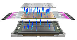
Avicena, headquartered in Sunnyvale, CA, announced today that the company will work with TSMC to optimize photodetector (PD) arrays for Avicena's revolutionary LightBundle microLED-based interconnects. LightBundle supports > 1Tbps/mm shoreline density and extends ultra-high density die-to-die (D2D) connections to > 10 meters at class-leading sub-pJ/bit energy efficiency. This will enable AI scale-up networks to support large clusters of GPUs across multiple racks, eliminating reach limitations of current copper interconnects while drastically reducing power consumption.
Increasingly sophisticated AI models are driving an unprecedented surge in demand for compute and memory performance, requiring interconnects with higher density, lower power, and longer reach for both processor-to-processor (P2P) and processor-to-memory (P2M) connectivity.
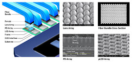
Increasingly sophisticated AI models are driving an unprecedented surge in demand for compute and memory performance, requiring interconnects with higher density, lower power, and longer reach for both processor-to-processor (P2P) and processor-to-memory (P2M) connectivity.


Intel's "Nova Lake" Processors Reportedly Slated for TSMC's 2nm Node
TSMC is pushing forward its plans to make 2 nm process chips in large quantities in the second half of the year, with major customer developments coming to light. After AMD placed its order, reports suggest Intel has also become one of TSMC's first 2 nm customers aiming to use this cutting-edge technology for its next-gen desktop processors. Intel, already a big TSMC customer for advanced processes sent out key compute tiles for its Core Ultra processors to TSMC using different processes like N3B, N5P, and N6. To be exact, these were Intel Core Ultra 200V "Lunar Lake" series laptop processors and Core Ultra 200S "Arrow Lake" series. While both companies didn't comment on the latest news, industry talk hints that they're cooperating on Intel's upcoming Nova Lake desktop processor set to launch next year (rumors suggest that it could be the Compute Tile). With the codename "NVL-S" Nova Lake combines two groups of eight high-performance "Coyote Cove" P-cores with 16 "Arctic Wolf" E-cores. It also includes four ultra-low-power LPE cores in a separate SoC tile. It is expected that Nova Lake-S will use LGA 1954, which has 1,954 active lands and might have more than 2,000 total pads when you count debug pins.
TSMC's work on 2 nm technology is moving forward as expected. The company uses first-generation nanochip transistor technology to boost performance and reduce power consumption across process nodes with big clients finishing designing silicon IPs and starting validation steps. AMD shared that its next EPYC "Venice" chip will be the first high-performance computing processor to use TSMC's 2 nm process. AMD validated it at TSMC's Arizona plant and is on track to launch it in 2026. Also, word has it that Apple's future iPhone 18 lineup will have its A20 chip made with the same TSMC 2 nm process.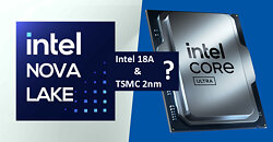
TSMC's work on 2 nm technology is moving forward as expected. The company uses first-generation nanochip transistor technology to boost performance and reduce power consumption across process nodes with big clients finishing designing silicon IPs and starting validation steps. AMD shared that its next EPYC "Venice" chip will be the first high-performance computing processor to use TSMC's 2 nm process. AMD validated it at TSMC's Arizona plant and is on track to launch it in 2026. Also, word has it that Apple's future iPhone 18 lineup will have its A20 chip made with the same TSMC 2 nm process.


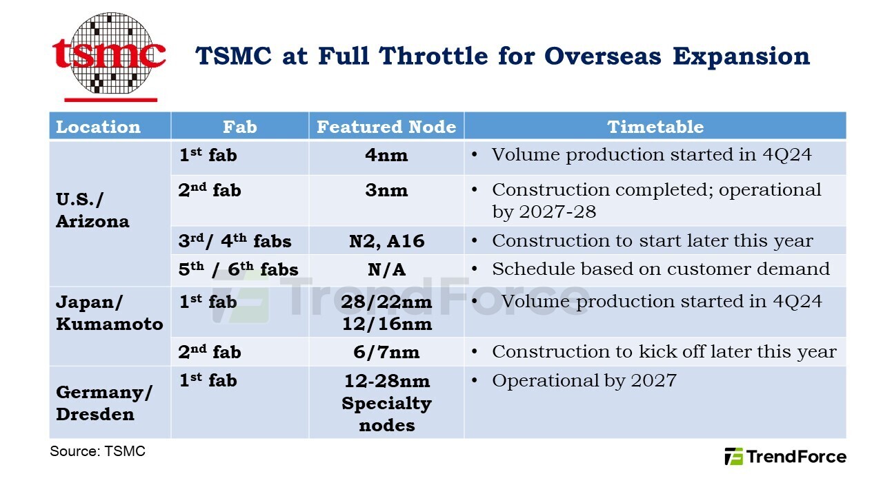
TSMC Expands U.S. Footprint with Two New Fabs in Arizona
TSMC is speeding up its plans to grow worldwide, the company's Chairman, C.C. Wei is announcing they'll start building their third and fourth fabs in Arizona later this year. This comes after TSMC finished constructing the second Arizona plant while the first fab started volume production in Q4 2024. TSMC wants to open its second factory about six months earlier than planned due to increasing customer demand. The first factory will make 4 nm chips, the second will target 3 nm chips, and the newer ones will work on even smaller N2 and A16 nodes. This rapid expansion is part of TSMC's additional $100 billion investment to build five more semiconductor plants and a research center in the U.S. In total, TSMC will invest $165 billion in the United States.
Besides its US operations, TSMC keeps pushing forward with its worldwide manufacturing plans. Wei dismissed rumors of setbacks at the company's upcoming Kumamoto plant in Japan. He confirmed that their first fab started mass production in late 2024, achieving excellent yields. They plan to begin building a second Japanese facility this year, once the infrastructure is ready. The company's European expansion in Dresden is also on track, with strong backing from both the European Commission and the German federal government. They broke ground at the Dresden site in August 2024 as Europe's first FinFET-capable dedicated foundry operation.

Besides its US operations, TSMC keeps pushing forward with its worldwide manufacturing plans. Wei dismissed rumors of setbacks at the company's upcoming Kumamoto plant in Japan. He confirmed that their first fab started mass production in late 2024, achieving excellent yields. They plan to begin building a second Japanese facility this year, once the infrastructure is ready. The company's European expansion in Dresden is also on track, with strong backing from both the European Commission and the German federal government. They broke ground at the Dresden site in August 2024 as Europe's first FinFET-capable dedicated foundry operation.

AMD Faces $800M Loss from U.S. Chip Export Curbs to China
AMD revealed today that it anticipates charges of up to $800 million following the Trump administration's latest crackdown on exports of advanced processors to China. The company confirmed that these new rules affect its MI308 product line. The U.S. Commerce Department declared on Tuesday that it was putting in place new licensing requirements impacting several high-performance chips, including NVIDIA's H20, AMD's MI308, and similar products. This regulatory move comes at a high price for AMD, as China stands as its second-biggest market in 2024 with about $6.23 billion in revenue, over 24% of the company's total sales.
AMD's regulatory filing reveals that the company faces $800 million in charges due to inventory issues, purchase commitments, and needed reserves. AMD "expects to apply for licenses but there is no assurance that licenses will be granted,". This uncertainty grows when we consider what Jefferies analysts pointed out on Tuesday: the U.S. has never agreed on licenses for graphics processor unit shipments to China. This news comes right after NVIDIA's announcement that it would take $5.5 billion in charges because of the same export rules. As a result, AMD and NVIDIA stocks were dropping by more than 5%.
AMD's regulatory filing reveals that the company faces $800 million in charges due to inventory issues, purchase commitments, and needed reserves. AMD "expects to apply for licenses but there is no assurance that licenses will be granted,". This uncertainty grows when we consider what Jefferies analysts pointed out on Tuesday: the U.S. has never agreed on licenses for graphics processor unit shipments to China. This news comes right after NVIDIA's announcement that it would take $5.5 billion in charges because of the same export rules. As a result, AMD and NVIDIA stocks were dropping by more than 5%.

Tariffs Push US Wafer Fab Equipment Costs Up 15% for Domestic Fabs
As the US works to bring more semiconductor manufacturing back home, the machines needed to turn silicon into the world's most advanced processors are becoming pricier and harder to get, thanks to tariffs. Foundries building new fabs report that the specialized equipment they rely on, everything from extreme ultraviolet (EUV) lithography steppers to chemical vapor deposition chambers, carries a roughly 15% premium compared with similar gear sold overseas. Several forces are at play. The raw materials, high‑grade quartz for vacuum enclosures, and exotic metal alloys for precision optics have climbed in price. At the same time, key components like ultra‑accurate motion stages and alignment sensors are in short supply, sometimes stretching lead times for critical subsystems well beyond 18 months. For a fab racing to move from a 7 nm to a 5 nm process, those delays can mean missing tight ramp‑up targets and pushing out product launches.
Smaller chipmakers feel the squeeze the hardest. With fewer orders to negotiate volume discounts, second‑tier foundries may see their capital budgets balloon by 20 percent or more. In response, some are taking a mixed approach, sourcing commoditized tools such as oxidation furnaces and rapid thermal processors from multiple suppliers while reserving single‑vendor deals for high‑stakes systems like EUV scanners. Government support through the CHIPS Act offers a partial safety net, helping to subsidize capital expenditures. Yet even with grants and tax credits, the challenges will remain. Success will hinge on tight coordination between fabs, equipment makers, and policymakers to tame rising costs, shorten delivery schedules, and keep America's chip renaissance on track.
Smaller chipmakers feel the squeeze the hardest. With fewer orders to negotiate volume discounts, second‑tier foundries may see their capital budgets balloon by 20 percent or more. In response, some are taking a mixed approach, sourcing commoditized tools such as oxidation furnaces and rapid thermal processors from multiple suppliers while reserving single‑vendor deals for high‑stakes systems like EUV scanners. Government support through the CHIPS Act offers a partial safety net, helping to subsidize capital expenditures. Yet even with grants and tax credits, the challenges will remain. Success will hinge on tight coordination between fabs, equipment makers, and policymakers to tame rising costs, shorten delivery schedules, and keep America's chip renaissance on track.


Google Unveils Seventh-Generation AI Processor: Ironwood
Google has rolled out its seventh-generation AI chip, Ironwood, which aims to boost AI application performance. This processor focuses on "inference" computing—the quick calculations needed for chatbot answers and other AI outputs. Ironwood stands as one of the few real options to NVIDIA's leading AI processors coming from Google's ten-year multi-billion-dollar push to develop it. These tensor processing units (TPUs) are exclusively available through Google's cloud service or to its internal engineers.
According to Google Vice President Amin Vahdat, Ironwood combines functions from previously separate designs while increasing memory capacity. The chip can operate in groups of up to 9,216 processors and delivers twice the performance-per-energy ratio compared to last year's Trillium chip. When configured in pods of 9,216 chips, Ironwood delivers 42.5 Exaflops of computing power. This is more than 24 times the computational capacity of El Capitan, currently the world's largest supercomputer, which provides only 1.7 Exaflops per pod.

According to Google Vice President Amin Vahdat, Ironwood combines functions from previously separate designs while increasing memory capacity. The chip can operate in groups of up to 9,216 processors and delivers twice the performance-per-energy ratio compared to last year's Trillium chip. When configured in pods of 9,216 chips, Ironwood delivers 42.5 Exaflops of computing power. This is more than 24 times the computational capacity of El Capitan, currently the world's largest supercomputer, which provides only 1.7 Exaflops per pod.


Tenstorrent Launches Blackhole Developer Products at Tenstorrent Dev Day
Tenstorrent launched the next generation Blackhole chip family today at their DevDay event in San Francisco. Featuring all new RISC-V cores, Blackhole is built to handle massive AI workloads efficiently and offers an infinitely scalable solution.
Blackhole products are now available for order on tenstorrent.com:


Blackhole products are now available for order on tenstorrent.com:
- Blackhole p100, powered by one processor without Ethernet, active-cooled: available for $999
- Blackhole p150, powered by one processor with Ethernet, and available in passive-, active-, and liquid-cooled variants: available for $1,299
- TT-Quiet box, a liquid-cooled desktop workstation powered by 4 Blackhole processors: available for $11,999


GUC Announces Tape-Out of the World's First HBM4 IP on TSMC N3P
Global Unichip Corp. (GUC), the Advanced ASIC Leader, announced today that it has successfully taped-out the world's first HBM4 controller and PHY IP. This test chip was implemented using TSMC's cutting-edge N3P process technology and CoWoS -R advanced packaging technology.
The HBM4 IP supports data rates of up to 12 Gbps under all operating conditions. By leveraging a proprietary interposer layout, GUC has optimized signal integrity (SI) and power integrity (PI) to achieve these high speeds for all types of CoWoS technology. Comparing with HBM3, GUC's HBM4 PHY delivers 2.5x bandwidth while improving 1.5x power efficiency and 2x area efficiency. In line with previous GUC HBM, GLink, and UCIe IPs, this HBM4 IP integrates proteanTecs' interconnect monitoring solution to provide high visibility for testing and characterizing the PHY while improving in-field performance and reliability for end products.
The HBM4 IP supports data rates of up to 12 Gbps under all operating conditions. By leveraging a proprietary interposer layout, GUC has optimized signal integrity (SI) and power integrity (PI) to achieve these high speeds for all types of CoWoS technology. Comparing with HBM3, GUC's HBM4 PHY delivers 2.5x bandwidth while improving 1.5x power efficiency and 2x area efficiency. In line with previous GUC HBM, GLink, and UCIe IPs, this HBM4 IP integrates proteanTecs' interconnect monitoring solution to provide high visibility for testing and characterizing the PHY while improving in-field performance and reliability for end products.

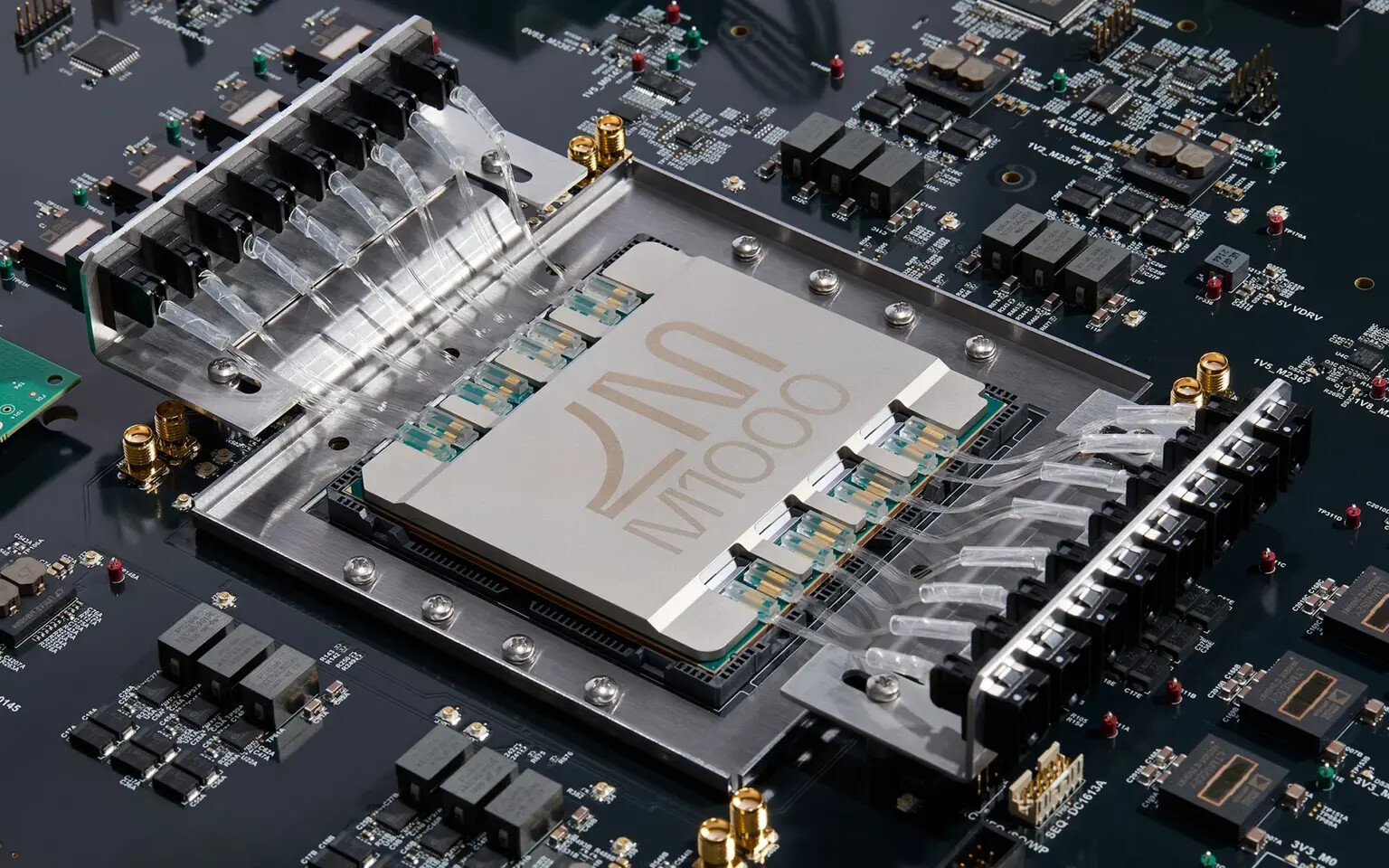
Lightmatter Unveils Passage M1000 Photonic Superchip
Lightmatter, the leader in photonic supercomputing, today announced Passage M1000, a groundbreaking 3D Photonic Superchip designed for next-generation XPUs and switches. The Passage M1000 enables a record-breaking 114 Tbps total optical bandwidth for the most demanding AI infrastructure applications. At more than 4,000 square millimeters, the M1000 reference platform is a multi-reticle active photonic interposer that enables the world's largest die complexes in a 3D package, providing connectivity to thousands of GPUs in a single domain.
In existing chip designs, interconnects for processors, memory, and I/O chiplets are bandwidth limited because electrical input/output (I/O) connections are restricted to the edges of these chips. The Passage M1000 overcomes this limitation by unleashing electro-optical I/O virtually anywhere on its surface for the die complex stacked on top. Pervasive interposer connectivity is enabled by an extensive and reconfigurable waveguide network that carries high-bandwidth WDM optical signals throughout the M1000. With fully integrated fiber attachment supporting an unprecedented 256 fibers, the M1000 delivers an order of magnitude higher bandwidth in a smaller package size compared to conventional Co-Packaged Optics (CPO) and similar offerings.

In existing chip designs, interconnects for processors, memory, and I/O chiplets are bandwidth limited because electrical input/output (I/O) connections are restricted to the edges of these chips. The Passage M1000 overcomes this limitation by unleashing electro-optical I/O virtually anywhere on its surface for the die complex stacked on top. Pervasive interposer connectivity is enabled by an extensive and reconfigurable waveguide network that carries high-bandwidth WDM optical signals throughout the M1000. With fully integrated fiber attachment supporting an unprecedented 256 fibers, the M1000 delivers an order of magnitude higher bandwidth in a smaller package size compared to conventional Co-Packaged Optics (CPO) and similar offerings.


xMEMS Introduces Lassen, Its First "Amplifier-Less" High-Performance MEMS Tweeter
xMEMS Labs, developers of the foremost platform for piezoMEMS innovation and creators of the world's leading all-silicon micro speakers, today announced xMEMS Lassen, the company's newest innovation for delivering micro fidelity (µFidelity) audio to mass-market consumer earbuds.
Responding to industrywide praise and enthusiastic reviews of xMEMS speaker technology for creating the highest quality sound, xMEMS has introduced Lassen, a lower cost all-silicon micro tweeter solution for TWS (True Wireless Stereo) earbuds.
Responding to industrywide praise and enthusiastic reviews of xMEMS speaker technology for creating the highest quality sound, xMEMS has introduced Lassen, a lower cost all-silicon micro tweeter solution for TWS (True Wireless Stereo) earbuds.

Rapidus Announces Strategic Partnership with Quest Global to Enable Advanced 2nm Solutions
Rapidus Corporation, a manufacturer of advanced logic semiconductors, today announced that it signed a Memorandum of Cooperation with Quest Global Services PTE. Ltd. As part of the agreement, Rapidus will become Quest Global's new semiconductor foundry partner, enabling it to provide a wide range of solutions to its customers. Quest Global customers will be able to leverage Rapidus' 2 nm gate-all-around (GAA) manufacturing process to develop engineering design and manufacturing solutions that will support growing industry demand for low-power artificial intelligence (AI) semiconductors. Together, the two companies will deliver transformational silicon solutions as a virtual integrated device manufacturer (IDM) model for fabless companies.
The AI semiconductor industry is in its early stages, with applications just beginning to emerge and new entrants quickly coming to market. Customers will shift from general-purpose AI semiconductors to dedicated designs that reduce power consumption and maximize performance. To support these industry requirements, customers will engage design firms focused on providing custom solutions, such as Quest Global, while also collaborating with semiconductor foundries, like Rapidus, that can manufacture dedicated semiconductors with a short turnaround time.

The AI semiconductor industry is in its early stages, with applications just beginning to emerge and new entrants quickly coming to market. Customers will shift from general-purpose AI semiconductors to dedicated designs that reduce power consumption and maximize performance. To support these industry requirements, customers will engage design firms focused on providing custom solutions, such as Quest Global, while also collaborating with semiconductor foundries, like Rapidus, that can manufacture dedicated semiconductors with a short turnaround time.


NVIDIA Plans US Supply Chain Investment Worth Hundreds of Billions, "Blackwell" Already Manufactured in Arizona
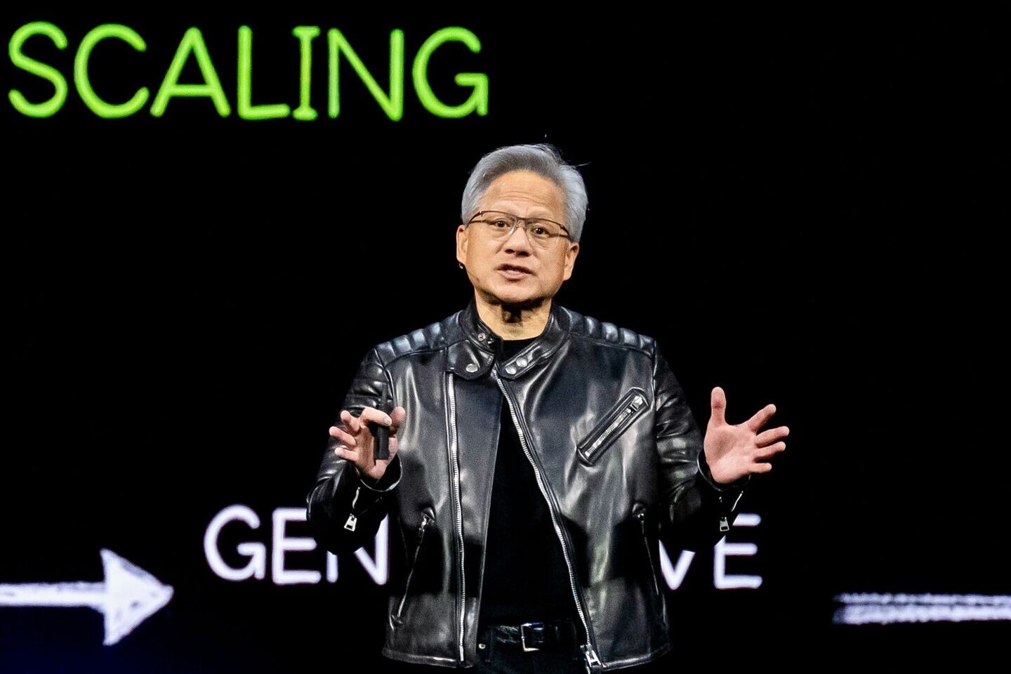
NVIDIA's CEO Jensen Huang made some interesting commentary for the Financial Times, stating that the company will procure over half a trillion US Dollars worth of electronics over the next four years, and it it plans to keep hundreds of billions from the supply chain procurement in the US. "Overall, we will procure, over the course of the next four years, probably half a trillion dollars worth of electronics in total. And I think we can easily see ourselves manufacturing several hundred billion of it here in the US," said Jensen for FT. NVIDIA currently manufactures its silicon at TSMC's facilities, as well as electronics like motherboards and servers at Foxconn. However, the geopolitical situation is making NVIDIA reconsider its supply chain dependencies, and the company is looking for more US-based manufacturing.
NVIDIA confirmed that its latest "Blackwell" series of GPUs, including the latest Blackwell Ultra, are being manufactured at TSMC's Arizona facilities. TSMC announced a $100 billion investment in its Arizona expansion, and NVIDIA is ready to take up more of TSMC's capacity to meet its ever-growing demand for GPUs. During the GTC 2025 event, Jensen noted that only four cloud service providers will use 3.6 million GPUs this year. That is without any AI labs and enterprises, which are massive consumers of GPUs (xAI only has 200,000 GPU clusters). To continue manufacturing excellence so customers won't suffer, NVIDIA is also looking at other options for supply chain manufacturing partners. Intel, the only US-based company capable of producing advanced silicon, is a potential target for NVIDIA. "We evaluate their foundry technology on a regular basis, and we are ongoing in doing that... We look for opportunities to be a customer of theirs... I have every confidence that Intel can do it," added Jensen, who also stated that NVIDIA is interested in silicon manufacturing and chip packaging services, as Intel's Foveros 3D packaging and other technologies are attractive for Team Green.
NVIDIA confirmed that its latest "Blackwell" series of GPUs, including the latest Blackwell Ultra, are being manufactured at TSMC's Arizona facilities. TSMC announced a $100 billion investment in its Arizona expansion, and NVIDIA is ready to take up more of TSMC's capacity to meet its ever-growing demand for GPUs. During the GTC 2025 event, Jensen noted that only four cloud service providers will use 3.6 million GPUs this year. That is without any AI labs and enterprises, which are massive consumers of GPUs (xAI only has 200,000 GPU clusters). To continue manufacturing excellence so customers won't suffer, NVIDIA is also looking at other options for supply chain manufacturing partners. Intel, the only US-based company capable of producing advanced silicon, is a potential target for NVIDIA. "We evaluate their foundry technology on a regular basis, and we are ongoing in doing that... We look for opportunities to be a customer of theirs... I have every confidence that Intel can do it," added Jensen, who also stated that NVIDIA is interested in silicon manufacturing and chip packaging services, as Intel's Foveros 3D packaging and other technologies are attractive for Team Green.
Vietnam to Begin First Wafer Fab Construction, Eyes Semiconductor Leadership in the Coming Decade
Vietnam's government has approved its first wafer fab facility, with an investment of 12.8 trillion VND (approximately $500 million). The first phase of the facility, scheduled for completion by 2030, is designed to manufacture specialized chips for defense, AI, and other high-tech applications. The project will receive government backing through direct funding—covering up to 30% of the total investment, capped at 10 trillion VND—and tax incentives. A special steering committee headed by the Prime Minister has been tasked with overseeing the project's execution and resource allocation. The new fab is a critical component of Vietnam's long-term semiconductor strategy, a phased approach toward building a domestic ecosystem for chip design, manufacturing, and testing. The current investment is modest compared to the typical costs of advanced wafer fabs, which can reach up to $50 billion.
Nonetheless, the project is a foundational, one-step-at-the-time move intended to spur further investments and technology transfer. Vietnamese officials have reportedly engaged in discussions with major international chip manufacturers—including US, South Korea, and Taiwan entities, such as GlobalFoundries and Powerchip Semiconductor Manufacturing Corp—to explore potential collaborative opportunities. Vietnam already hosts 174 semiconductor-related projects, predominantly focused on chip packaging and testing, in which global companies like Intel and Amkor have established significant operations. The second phase, from 2030-2040, envisions Vietnam emerging as a worldwide center for electronics and semiconductors. By expanding to at least 200 design companies, establishing two semiconductor chip manufacturing plants, and creating 15 packaging and testing facilities, the country intends to gradually develop independent semiconductor product design and production capabilities.
Nonetheless, the project is a foundational, one-step-at-the-time move intended to spur further investments and technology transfer. Vietnamese officials have reportedly engaged in discussions with major international chip manufacturers—including US, South Korea, and Taiwan entities, such as GlobalFoundries and Powerchip Semiconductor Manufacturing Corp—to explore potential collaborative opportunities. Vietnam already hosts 174 semiconductor-related projects, predominantly focused on chip packaging and testing, in which global companies like Intel and Amkor have established significant operations. The second phase, from 2030-2040, envisions Vietnam emerging as a worldwide center for electronics and semiconductors. By expanding to at least 200 design companies, establishing two semiconductor chip manufacturing plants, and creating 15 packaging and testing facilities, the country intends to gradually develop independent semiconductor product design and production capabilities.

US Self-Sufficiency of Semiconductors Unlikely According to Japanese Expert
According to Akira Amari, a Japanese politician and semiconductor industry expert, it's unlikely that the US will ever reach self-sufficiency when it comes to semiconductor production. This has nothing to do with foundries, as the US might manage to be self-sufficient in terms or raw chip production needs, but the country is said to be unlikely to be able to reach a complete supply chain of everything else needed to produce the chips. Countries like Japan, Taiwan, the Netherlands, Belgium, South Korea and more are heavily invested in supplying not only components needed to produce semiconductors, but also machinery and chemicals.
Amari is suggesting that these countries should form a co-operative alliance to help strengthen their supply chains at home, rather than putting all eggs in one basket to try and appease the US. This statement comes after TSMC promised to invest an additional US$100 billion over an unspecified time frame in the US. Time will tell if he's right or not, but it's unlikely that any country will ever be self-sufficient when it comes to making semiconductors, regardless of how big they are or what natural resources they have access to locally.
Amari is suggesting that these countries should form a co-operative alliance to help strengthen their supply chains at home, rather than putting all eggs in one basket to try and appease the US. This statement comes after TSMC promised to invest an additional US$100 billion over an unspecified time frame in the US. Time will tell if he's right or not, but it's unlikely that any country will ever be self-sufficient when it comes to making semiconductors, regardless of how big they are or what natural resources they have access to locally.

Global Top 10 IC Design Houses See 49% YoY Growth in 2024, NVIDIA Commands Half the Market
TrendForce reveals that the combined revenue of the world's top 10 IC design houses reached approximately US$249.8 billion in 2024, marking a 49% YoY increase. The booming AI industry has fueled growth across the semiconductor sector, with NVIDIA leading the charge, posting an astonishing 125% revenue growth, widening its lead over competitors, and solidifying its dominance in the IC industry.
Looking ahead to 2025, advancements in semiconductor manufacturing will further enhance AI computing power, with LLMs continuing to emerge. Open-source models like DeepSeek could lower AI adoption costs, accelerating AI penetration from servers to personal devices. This shift positions edge AI devices as the next major growth driver for the semiconductor industry.
Looking ahead to 2025, advancements in semiconductor manufacturing will further enhance AI computing power, with LLMs continuing to emerge. Open-source models like DeepSeek could lower AI adoption costs, accelerating AI penetration from servers to personal devices. This shift positions edge AI devices as the next major growth driver for the semiconductor industry.

4Q24 Global Top 10 Foundries Set New Revenue Record, TSMC Leads in Advanced Process Nodes
TrendForce's latest research reveals that the global foundry industry exhibited a polarized trend in 4Q24. Advanced process nodes benefited from strong demand in AI servers, flagship smartphone application processors (APs), and new PC platforms, driving high-value wafer shipments. This growth helped offset the slowdown in mature process demand, allowing the top 10 foundries to achieve nearly 10% QoQ revenue growth, reaching US$38.48 billion, and marking another industry record.
TrendForce notes that new U.S. trade tariffs under the Trump administration have started affecting the foundry industry. A surge in recent orders for TVs, PCs, and notebooks bound for the U.S. in 4Q24 is expected to extend into 1Q25. Additionally, China's consumer subsidy program—introduced in late 2024—has spurred early inventory restocking among upstream customers. Combined with persistent demand for TSMC's AI-related chips and advanced packaging, these factors suggest that despite Q1 being a seasonally weak quarter, foundry revenue will only decline slightly.
TrendForce notes that new U.S. trade tariffs under the Trump administration have started affecting the foundry industry. A surge in recent orders for TVs, PCs, and notebooks bound for the U.S. in 4Q24 is expected to extend into 1Q25. Additionally, China's consumer subsidy program—introduced in late 2024—has spurred early inventory restocking among upstream customers. Combined with persistent demand for TSMC's AI-related chips and advanced packaging, these factors suggest that despite Q1 being a seasonally weak quarter, foundry revenue will only decline slightly.

Codasip Selected to Design a High-End RISC-V Processor for the EU-Funded DARE Project
Codasip, the European RISC-V leader, announced that it has been selected to provide a general purpose, high-end processor as part of the large-scale European supercomputing project Digital Autonomy with RISC-V in Europe (DARE).
DARE is set to build a supercomputing compute stack, featuring high-performance and energy-efficient RISC-V-based processors and accelerators designed and developed in Europe. The European Union has committed 240 million Euros in funding for the first 3-year program phase. The selected partners will leverage hardware/software co-design to achieve competitive performance and efficiency.
DARE is set to build a supercomputing compute stack, featuring high-performance and energy-efficient RISC-V-based processors and accelerators designed and developed in Europe. The European Union has committed 240 million Euros in funding for the first 3-year program phase. The selected partners will leverage hardware/software co-design to achieve competitive performance and efficiency.

SK keyfoundry Launches 3D Hall-effect Sensor Technology Capable of Measuring Speed and Direction
SK keyfoundry, an 8-inch pure-play foundry in Korea, announced today that it offers a new 3D Hall-effect sensor technology that can measure speed and direction through three-dimensional magnetic field detection for its foundry customers.
The Hall-effect sensor is a device that measures the strength of a magnetic field using the Hall-effect, which detects the voltage difference generated when a conductor or semiconductor passes through a magnetic field. The measured magnetic field is utilized in applications that leverage the position, speed, rotation, direction, and current of devices.
The Hall-effect sensor is a device that measures the strength of a magnetic field using the Hall-effect, which detects the voltage difference generated when a conductor or semiconductor passes through a magnetic field. The measured magnetic field is utilized in applications that leverage the position, speed, rotation, direction, and current of devices.

Microchip Technology Releases MPLAB PICkit Basic Debugger
To make its robust programming and debugging capabilities accessible to a wider range of engineers, Microchip Technology has launched the MPLAB PICkit Basic in-circuit debugger as a cost-effective, powerful solution for engineers at various levels. Unlike other complex and expensive debuggers, this budget-friendly device offers high-speed USB 2.0 connectivity, CMSIS-DAP support, compatibility with various Integrated Development Environments (IDEs) and compatibility with a broad range of microcontrollers. The tool's versatility allows developers to use the debugger across various projects and platforms—including VS Code ecosystems—to simplify the workflow and reduce the need for multiple tools.
Key features:


Key features:
- USB Type-C Cable: The MPLAB PICkit Basic programmer debugger uses a USB Type-C cable, which is modern, widely adopted and easy to use. The USB-C connection helps promote better connectivity, faster data transfer and a more reliable connection, reducing the hassle of dealing with outdated or incompatible cables.


Marvell Demonstrates Industry's Leading 2nm Silicon for Accelerated Infrastructure
Marvell Technology, Inc., a leader in data infrastructure semiconductor solutions, has demonstrated its first 2 nm silicon IP for next-generation AI and cloud infrastructure. Produced on TSMC's 2 nm process, the working silicon is part of the Marvell platform for developing custom XPUs, switches and other technology to help cloud service providers elevate the performance, efficiency, and economic potential of their worldwide operations.
Given a projected 45% TAM growth annually, custom silicon is expected to account for approximately 25% of the market for accelerated compute by 20281.
Given a projected 45% TAM growth annually, custom silicon is expected to account for approximately 25% of the market for accelerated compute by 20281.

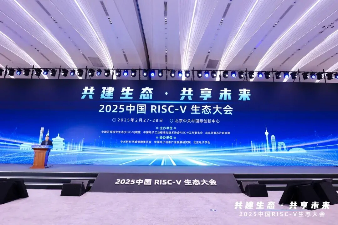
SOPHGO Unveils New Products at the 2025 China RISC-V Ecosystem Conference
On February 27-28, the 2025 China RISC-V Ecosystem Conference was grandly held at the Zhongguancun International Innovation Center in Beijing. As a core promoter in the RISC-V field, SOPHGO was invited to deliver a speech and prominently launch a series of new products based on the SG2044 chip, sharing the company's cutting-edge practices in the heterogeneous fusion of AI and RISC-V, and contributing to the vigorous development of the global open-source instruction set ecosystem. During the conference, SOPHGO set up a distinctive exhibition area that attracted many attendees from the industry to stop and watch.
Focusing on AI Integration, Leading Breakthroughs in RISC-V Technology
At the main forum of the conference, the Vice President of SOPHGO RISC-V delivered a speech titled "RISC-V Breakthroughs Driven by AI: Integration + Heterogeneous Innovation," where he elaborated on SOPHGO's innovative achievements in the deep integration of RISC-V architecture and artificial intelligence technology. He pointed out that current AI technological innovations are driving market changes, and the emergence of DeepSeek has ignited a trillion-level computing power market. The innovation of technical paradigms and the penetration of large models into various sectors will lead to an explosive growth in inference demand, resulting in changes in the structure of computing power demand. This will also reshape the landscape of the computing power market, bringing significant business opportunities to domestic computing power enterprises, while RISC-V high-performance computing is entering a fast track of development driven by AI.


GlobalFoundries and MIT Collaborate on Photonic AI Chips
GlobalFoundries (GF) and the Massachusetts Institute of Technology (MIT) today announced a new master research agreement to jointly pursue advancements and innovations for enhancing the performance and efficiency of critical semiconductor technologies. The collaboration will be led by MIT's Microsystems Technology Laboratories (MTL) and GF's research and development team, GF Labs.
With an initial research focus on AI and other applications, the first projects are expected to leverage GF's differentiated silicon photonics technology, which monolithically integrates RF SOI, CMOS and optical features on a single chip to realize power efficiencies for datacenters, and GF's 22FDX platform, which delivers ultra-low power consumption for intelligent devices at the edge.
With an initial research focus on AI and other applications, the first projects are expected to leverage GF's differentiated silicon photonics technology, which monolithically integrates RF SOI, CMOS and optical features on a single chip to realize power efficiencies for datacenters, and GF's 22FDX platform, which delivers ultra-low power consumption for intelligent devices at the edge.


Amazon Web Services Announces New Quantum Computing Chip
Today, Amazon Web Services (AWS) announced Ocelot, a new quantum computing chip that can reduce the costs of implementing quantum error correction by up to 90%, compared to current approaches. Developed by the team at the AWS Center for Quantum Computing at the California Institute of Technology, Ocelot represents a breakthrough in the pursuit to build fault-tolerant quantum computers capable of solving problems of commercial and scientific importance that are beyond the reach of today's conventional computers.
AWS used a novel design for Ocelot's architecture, building error correction in from the ground up and using the 'cat qubit'. Cat qubits-named after the famous Schrödinger's cat thought experiment-intrinsically suppress certain forms of errors, reducing the resources required for quantum error correction. Through this new approach with Ocelot, AWS researchers have, for the first time, combined cat qubit technology and additional quantum error correction components onto a microchip that can be manufactured in a scalable fashion using processes borrowed from the microelectronics industry.

AWS used a novel design for Ocelot's architecture, building error correction in from the ground up and using the 'cat qubit'. Cat qubits-named after the famous Schrödinger's cat thought experiment-intrinsically suppress certain forms of errors, reducing the resources required for quantum error correction. Through this new approach with Ocelot, AWS researchers have, for the first time, combined cat qubit technology and additional quantum error correction components onto a microchip that can be manufactured in a scalable fashion using processes borrowed from the microelectronics industry.


Open Compute Project Foundation and JEDEC Announce New Chiplet Design Kits
Today, the Open Compute Project Foundation (OCP), the nonprofit organization bringing hyperscale innovations to all, and JEDEC Solid State Technology Association, the global leader in the development of standards for the microelectronics industry, announce the availability of new Chiplet Design Kits for use with today's EDA tools covering Assembly, Substrate, Material and Test developed in collaboration within the OCP Open Chiplet Economy Project. Leveraging the alliance between OCP and JEDEC, these design kits are now part of the Global Worldwide Standard JEDEC JEP30: Part Model Guidelines.
The release of the Assembly, Substrate, Material, and Test Design Kits build on earlier joint efforts between the OCP and JEDEC integrating OCP Chiplet Data Extensible Markup Language (CDXML) specification into JEDEC JEP30: Part Model Guidelines, enabling Chiplet builders to provide electronically a standardized Chiplet part description to their customers, paving the way for automating System-in-Package (SiP) design and build using Chiplets.

The release of the Assembly, Substrate, Material, and Test Design Kits build on earlier joint efforts between the OCP and JEDEC integrating OCP Chiplet Data Extensible Markup Language (CDXML) specification into JEDEC JEP30: Part Model Guidelines, enabling Chiplet builders to provide electronically a standardized Chiplet part description to their customers, paving the way for automating System-in-Package (SiP) design and build using Chiplets.


Baya Systems and Semidynamics Collaborate to Accelerate RISC-V System-on-Chip Development
Baya Systems, a leader in system IP technology that empowers the acceleration of intelligent compute, and Semidynamics, a provider of fully customizable high-bandwidth and high-performance RISC-V processor IP, today announced a collaboration to boost innovation in development of hyper-efficient, next-generation platforms for artificial intelligence (AI), machine learning (ML) and high-performance computing (HPC) applications.
The collaboration integrates Semidynamics' family of 64-bit RISC-V processor IP cores, known for their exceptional memory bandwidth and configurability, with Baya Systems' innovative WeaveIP Network on Chip (NoC) system IP. WeaveIP is engineered for ultra-efficient, high-bandwidth, and low-latency data transport, crucial for the demands of modern workloads. Complementing this is Baya Systems' software-driven WeaverPro platform, which enables rapid system-level optimization, ensuring that key performance indicators (KPIs) are met based on real-world workloads while providing unparalleled design flexibility for future advancements.
The collaboration integrates Semidynamics' family of 64-bit RISC-V processor IP cores, known for their exceptional memory bandwidth and configurability, with Baya Systems' innovative WeaveIP Network on Chip (NoC) system IP. WeaveIP is engineered for ultra-efficient, high-bandwidth, and low-latency data transport, crucial for the demands of modern workloads. Complementing this is Baya Systems' software-driven WeaverPro platform, which enables rapid system-level optimization, ensuring that key performance indicators (KPIs) are met based on real-world workloads while providing unparalleled design flexibility for future advancements.

Apr 24th, 2025 13:51 EDT
change timezone
Latest GPU Drivers
New Forum Posts
- Choosing an Internal HDD (2)
- New GPU 5070 Ti or better CPU Ryzen7 7800X3D ? (18)
- Companies should be called out for this (91)
- Are the 8 GB cards worth it? (160)
- To distill or not distill what say ye? (99)
- Do you use Linux? (592)
- I dont understand the phone OS world..... (32)
- 5060 Ti 8GB DOA (265)
- Thermal testing two different size Gigabyte 5070 Ti cards - huge differences (28)
- Asus Rx570 o4g cannot losd drivers error code 43 (15)
Popular Reviews
- NVIDIA GeForce RTX 5060 Ti 8 GB Review - So Many Compromises
- Colorful iGame B860M Ultra V20 Review
- ASUS GeForce RTX 5060 Ti TUF OC 16 GB Review
- ASRock X870E Taichi Lite Review
- Upcoming Hardware Launches 2025 (Updated Apr 2025)
- Sapphire Radeon RX 9070 XT Pulse Review
- Sapphire Radeon RX 9070 XT Nitro+ Review - Beating NVIDIA
- Crucial CUDIMM DDR5-6400 128 GB CL52 Review
- AMD Ryzen 7 9800X3D Review - The Best Gaming Processor
- NVIDIA GeForce RTX 5060 Ti PCI-Express x8 Scaling
Controversial News Posts
- NVIDIA GeForce RTX 5060 Ti 16 GB SKU Likely Launching at $499, According to Supply Chain Leak (182)
- NVIDIA Sends MSRP Numbers to Partners: GeForce RTX 5060 Ti 8 GB at $379, RTX 5060 Ti 16 GB at $429 (127)
- NVIDIA Launches GeForce RTX 5060 Series, Beginning with RTX 5060 Ti This Week (115)
- Nintendo Confirms That Switch 2 Joy-Cons Will Not Utilize Hall Effect Stick Technology (105)
- Nintendo Switch 2 Launches June 5 at $449.99 with New Hardware and Games (99)
- Sony Increases the PS5 Pricing in EMEA and ANZ by Around 25 Percent (85)
- NVIDIA PhysX and Flow Made Fully Open-Source (77)
- Windows Notepad Gets Microsoft Copilot Integration (75)