News Posts matching #chip

Return to Keyword Browsing

Mobilint Debuts New AI Chips at Silicon Valley Summit

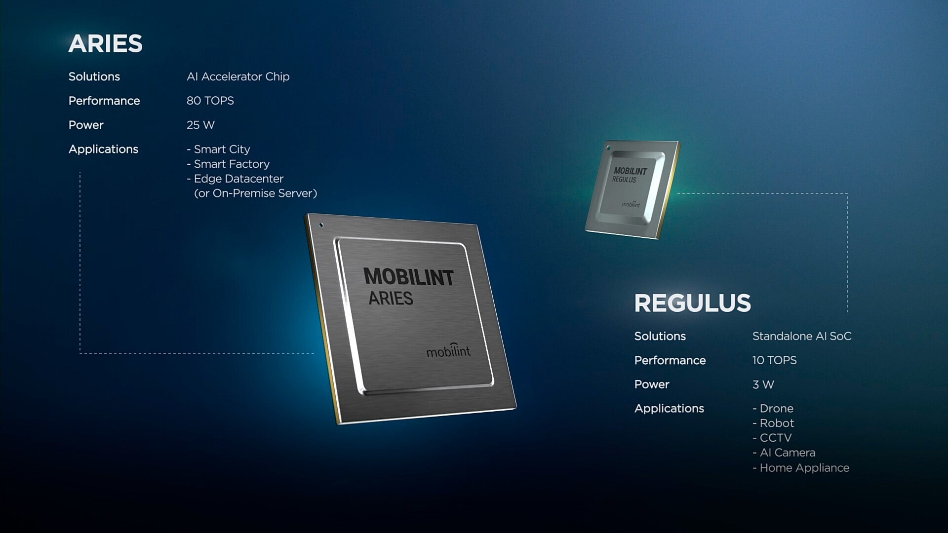
Mobilint, an edge AI chip company led by CEO Dongjoo Shin, is set to make waves at the upcoming AI Hardware & Edge AI Summit 2024 in Silicon Valley. The three-day event, starting on September 10th, will showcase Mobilint's latest innovations in AI chip technology. The company will demonstrate live demos of its high-efficiency SoC 'REGULUS' for on-device AI and high-performance acceleration chip 'ARIES' for on-premises AI.

The AI Hardware Summit is an annual event where global IT giants such as Microsoft, NVIDIA, Google, Meta, and AMD, along with prominent startups, gather to share their developments in AI and machine learning. This year's summit features world-renowned AI experts as speakers, including Andrew Ng, CEO of Landing AI, and Mark Russinovich, CTO of Microsoft Azure.

Coalition Formed to Accelerate the Use of Glass Substrates for Advanced Chips and Chiplets

E&R Engineering Corp. hosted an event on August 28, 2024, in Taipei, Taiwan, where they launched the "E-Core System." This initiative, a combination of "E&R" and "Glass Core" inspired by the sound of "Ecosystem," led to the establishment of the "Glass Substrate Supplier E-Core System Alliance." The alliance aims to combine expertise to promote comprehensive solutions, providing equipment and materials for next-generation advanced packaging with glass substrates to both domestic and international customers.

E&R's E-Core Alliance includes Manz AG, Scientech for wet etching, HYAWEI OPTRONICS for AOI optical inspection, Lincotec, STK Corp., Skytech, Group Up for sputtering and ABF lamination equipment, and other key component suppliers such as HIWIN, HIWIN MIKROSYSTEM, Keyence Taiwan, Mirle Group, ACE PILLAR CHYI DING), and Coherent.

Chinese GPU Maker XCT Faces Financial Crisis and Legal Troubles

Xiangdixian Computing Technology (XCT), once hailed as China's answer to NVIDIA at its peak, is now grappling with severe financial difficulties and legal challenges. The company, which has developed its own line of GPUs based on the Tianjun chips, recently admitted that its progress in "development of national GPU has not yet fully met the company's expectations and is facing certain market adjustment pressures." Despite producing two desktop and one workstation GPU model, XCT has been forced to address rumors of its closure. The company has undergone significant layoffs, but it claims to have retained key research and development staff essential for GPU advancement. Adding to XCT's woes, investors have initiated legal proceedings against the company's founder, Tang Zhimin, claiming he failed to deliver on his commitment to raising 500 million Yuan in Series B funding.

Among the complainants is the state-owned Jiangsu Zhongde Services Trade Industry Investment Fund, which has filed a lawsuit against three companies under Zhimin's control. Further complicating matters, Capitalonline Data Service is reportedly suing XCT for unpaid debts totaling 18.8 million Yuan. There are also claims that the company's bank accounts have been frozen, potentially impeding its ability to continue operations. The situation is further complicated by allegations of corruption within China's semiconductor sector, with reports of executives misappropriating investment funds. With XCT fighting for survival through restructuring efforts, its fate hangs in the balance. Without securing additional funding soon, the company may be forced to close its doors, which will blow China's GPU aspirations.

Microsoft Unveils New Details on Maia 100, Its First Custom AI Chip

Microsoft provided a detailed view of Maia 100 at Hot Chips 2024, their initial specialized AI chip. This new system is designed to work seamlessly from start to finish, with the goal of improving performance and reducing expenses. It includes specially made server boards, unique racks, and a software system focused on increasing the effectiveness and strength of sophisticated AI services, such as Azure OpenAI. Microsoft introduced Maia at Ignite 2023, sharing that they had created their own AI accelerator chip. More information was provided earlier this year at the Build developer event. The Maia 100 is one of the biggest processors made using TSMC's 5 nm technology, designed for handling extensive AI tasks on Azure platform.

Maia 100 SoC architecture features:
  • A high-speed tensor unit (16xRx16) offers rapid processing for training and inferencing while supporting a wide range of data types, including low precision data types such as the MX data format, first introduced by Microsoft through the MX Consortium in 2023.
  • The vector processor is a loosely coupled superscalar engine built with custom instruction set architecture (ISA) to support a wide range of data types, including FP32 and BF16.
  • A Direct Memory Access (DMA) engine supports different tensor sharding schemes.
  • Hardware semaphores enable asynchronous programming on the Maia system.

FuriosaAI Unveils RNGD Power-Efficient AI Processor at Hot Chips 2024

Today at Hot Chips 2024, FuriosaAI is pulling back the curtain on RNGD (pronounced "Renegade"), our new AI accelerator designed for high-performance, highly efficient large language model (LLM) and multimodal model inference in data centers. As part of his Hot Chips presentation, Furiosa co-founder and CEO June Paik is sharing technical details and providing the first hands-on look at the fully functioning RNGD card.

With a TDP of 150 watts, a novel chip architecture, and advanced memory technology like HBM3, RNGD is optimized for inference with demanding LLMs and multimodal models. It's built to deliver high performance, power efficiency, and programmability all in a single product - a trifecta that the industry has struggled to achieve in GPUs and other AI chips.

xMEMS Introduces 1mm-Thin Active Micro-Cooling Fan on a Chip

xMEMS Labs, developers of the foremost platform for piezoMEMS innovation and creators of the world's leading all-silicon micro speakers, today announced its latest industry-changing innovation: the xMEMS XMC-2400 µCooling chip, the first-ever all-silicon, active micro-cooling fan for ultramobile devices and next-generation artificial intelligence (AI) solutions.

For the first time, with active, fan-based micro-cooling (µCooling) at the chip level, manufacturers can integrate active cooling into smartphones, tablets, and other advanced mobile devices with the silent, vibration-free, solid-state xMEMS XMC-2400 µCooling chip, which measures just 1-millimeter thin.

India Targets 2026 for Its First Domestic AI Chip Development

Ola, an Indian automotive company, is venturing into AI chip development with its artificial intelligence branch, Krutrim, planning to launch India's first domestically designed AI chip by 2026. The company is leveraging ARM architecture for this initiative. CEO Bhavish Aggarwal emphasizes the importance of India developing its own AI technology rather than relying on external sources.

While detailed specifications are limited, Ola claims these chips will offer competitive performance and efficiency. For manufacturing, the company plans to partner with a global tier I or II foundry, possibly TSMC or Samsung. "We are still exploring foundries, we will go with a global tier I or II foundry. Taiwan is a global leader, and so is Korea. I visited Taiwan a couple of months back and the ecosystem is keen on partnering with India," Aggarwal said.

Samsung to Install High-NA EUV Machines Ahead of TSMC in Q4 2024 or Q1 2025

Samsung Electronics is set to make a significant leap in semiconductor manufacturing technology with the introduction of its first High-NA 0.55 EUV lithography tool. The company plans to install the ASML Twinscan EXE:5000 system at its Hwaseong campus between Q4 2024 and Q1 2025, marking a crucial step in developing next-generation process technologies for logic and DRAM production. This move positions Samsung about a year behind Intel but ahead of rivals TSMC and SK Hynix in adopting High-NA EUV technology. The system is expected to be operational by mid-2025, primarily for research and development purposes. Samsung is not just focusing on the lithography equipment itself but is building a comprehensive ecosystem around High-NA EUV technology.

The company is collaborating with several key partners like Lasertec (developing inspection equipment for High-NA photomasks), JSR (working on advanced photoresists), Tokyo Electron (enhancing etching machines), and Synopsys (shifting to curvilinear patterns on photomasks for improved circuit precision). The High-NA EUV technology promises significant advancements in chip manufacturing. With an 8 nm resolution capability, it could make transistors about 1.7 times smaller and increase transistor density by nearly three times compared to current Low-NA EUV systems. However, the transition to High-NA EUV comes with challenges. The tools are more expensive, costing up to $380 million each, and have a smaller imaging field. Their larger size also requires chipmakers to reconsider fab layouts. Despite these hurdles, Samsung aims for commercial implementation of High-NA EUV by 2027.

Geekbench AI Hits 1.0 Release: CPUs, GPUs, and NPUs Finally Get AI Benchmarking Solution

Primate Labs, the developer behind the popular Geekbench benchmarking suite, has launched Geekbench AI—a comprehensive benchmark tool designed to measure the artificial intelligence capabilities of various devices. Geekbench AI, previously known as Geekbench ML during its preview phase, has now reached version 1.0. The benchmark is available on multiple operating systems, including Windows, Linux, macOS, Android, and iOS, making it accessible to many users and developers. One of Geekbench AI's key features is its multifaceted approach to scoring. The benchmark utilizes three distinct precision levels: single-precision, half-precision, and quantized data. This evaluation aims to provide a more accurate representation of AI performance across different hardware designs.

In addition to speed, Geekbench AI places a strong emphasis on accuracy. The benchmark assesses how closely each test's output matches the expected results, offering insights into the trade-offs between performance and precision. The release of Geekbench AI 1.0 brings support for new frameworks, including OpenVINO, ONNX, and Qualcomm QNN, expanding its compatibility across various platforms. Primate Labs has also implemented measures to ensure fair comparisons, such as enforcing minimum runtime durations for each workload. The company noted that Samsung and NVIDIA are already utilizing the software to measure their chip performance in-house, showing that adoption is already strong. While the benchmark provides valuable insights, real-world AI applications are still limited, and reliance on a few benchmarks may paint a partial picture. Nevertheless, Geekbench AI represents a significant step forward in standardizing AI performance measurement, potentially influencing future consumer choices in the AI-driven tech market. Results from the benchmark runs can be seen here.

Huawei Reportedly Developing New Ascend 910C AI Chip to Rival NVIDIA's H100 GPU

Amidst escalating tensions in the U.S.-China semiconductor industry, Huawei is reportedly working on a new AI chip called the Ascend 910C. This development appears to be the Chinese tech giant's attempt to compete with NVIDIA's AI processors in the Chinese market. According to a Wall Street Journal report, Huawei has begun testing the Ascend 910C with various Chinese internet and telecom companies to evaluate its performance and capabilities. Notable firms such as ByteDance, Baidu, and China Mobile are said to have received samples of the chip.

Huawei has reportedly informed its clients that the Ascend 910C can match the performance of NVIDIA's H100 chip. The company has been conducting tests for several weeks, suggesting that the new processor is nearing completion. The Wall Street Journal indicates that Huawei could start shipping the chip as early as October 2024. The report also mentions that Huawei and potential customers have discussed orders for over 70,000 chips, potentially worth $2 billion.

SiFive Announces Performance P870-D RISC-V Datacenter Processor

Today SiFive, Inc., the gold standard for RISC-V computing, announced its new SiFive Performance P870-D datacenter processor to meet customer requirements for highly parallelizable infrastructure workloads including video streaming, storage, and web appliances. When used in combination with products from the SiFive Intelligence product family, datacenter architects can also build an extremely high-performance, energy efficient compute subsystem for AI-powered applications.

Building on the success of the P870, the P870-D supports the open AMBA CHI protocol so customers have more flexibility to scale the number of clusters. This scalability allows customers to boost performance while minimizing power consumption. By harnessing a standard CHI bus, the P870-D enables SiFive's customers to scale up to 256 cores while harnessing industry-standard protocols, including Compute Express Link (CXL) and CHI chip to chip (C2C), to enable coherent high core count heterogeneous SoCs and chiplet configurations.

Akeana Exits Stealth Mode with Comprehensive RISC-V Processor Portfolio

Akeana, the company committed to driving dramatic change in semiconductor IP innovation and performance, has announced its official company launch approximately three years after its foundation, having raised over $100 million in capital, with support from A-list investors including Kleiner Perkins, Mayfield, and Fidelity. Today's launch marks the formal availability of the company's expansive line of IP solutions that are uniquely customizable for any workload or application.

Formed by the same team that designed Marvell's ThunderX2 server chips, Akeana offers a variety of IP solutions, including microcontrollers, Android clusters, AI vector cores and subsystems, and compute clusters for networking and data centers. Akeana moves the industry beyond the status quo of legacy vendors and architectures, like Arm, with equitable licensing options and processors that fill and exceed current performance gaps.

Samsung's 8-layer HBM3E Chips Pass NVIDIA's Tests

Samsung Electronics has achieved a significant milestone in its pursuit of supplying advanced memory chips for AI systems. Their latest fifth-generation high-bandwidth memory (HBM) chips, known as HBM3E, have finally passed all NVIDIA's tests. This approval will help Samsung in catching up with competitors SK Hynix and Micron in the race to provide HBM memory chips to NVIDIA. While a supply deal hasn't been finalized yet, deliveries are expected to start in late 2024.

However, it's worth noting that Samsung passed NVIDIA's tests for the eight-layer HBM3E chips while the more advanced twelve-layer version of the HBM3E chips is still struggling pass those tests. Both Samsung and NVIDIA declined to comment on these developments. Industry expert Dylan Patel notes that while Samsung is making progress, they're still behind SK Hynix, which is already preparing to ship its own twelve-layer HBM3E chips.

Silicon Motion Launches Power Efficient PCIe Gen 5 SSD Controller

Silicon Motion Technology Corporation, a global leader in designing and marketing NAND flash controllers for solid-state storage devices, today announced SM2508, the best power efficiency PCIe Gen 5 NVMe 2.0 client SSD controller for AI PCs and gaming consoles. It's the world's first PCIe Gen 5 client SSD controller using TSMC's 6 nm EUV process, offering a 50% reduction in power consumption compared to competitive offerings in the 12 nm process. With less than 7 W power consumption for the entire SSD, it delivers 1.7x better power efficiency than PCIe Gen 4 SSDs and up to 70% better than current competitive PCIe Gen 5 offerings on the market. Silicon Motion will be showcasing its SM2508 based SSD design and other innovations during the Future of Memory and Storage event from Aug. 6 to 8 at booth #315:

Silicon Motion's SM2508 is a superior-performance, low-power PCIe Gen 5 x4 NVMe 2.0 SSD controller designed for AI-capable PC notebooks. It supports eight NAND channels with up to 3,600 MT/s per channel, delivering sequential performance speeds of up to 14.5 GB/s and 13.6 GB/s and random performance speeds of up to 2.5M IOPS, providing up to 2x higher performance than PCIe Gen 4 products. The SM2508 maximizes PCIe Gen 5 performance with an impressive power consumption of approximately 3 W. It features Silicon Motion's proprietary 8th-generation NANDXtend technology, which includes an on-disk training algorithm designed to reduce ECC timing. This enhancement boosts performance and maximizes power efficiency while ensuring compatibility with the latest 3D TLC/QLC NAND technologies, enabling higher data density and meeting the evolving demands of next-generation AI PCs.

Ampere Announces 512-Core AmpereOne Aurora CPU for AI Computing

Ampere has announced a significant update to its product roadmap, highlighting the upcoming 512-core AmpereOne Aurora processor. This new chip is specifically designed to address the growing demands of cloud-native AI computing.

The newly announced AmpereOne Aurora 512 cores processor integrates AI acceleration and on-chip High Bandwidth Memory (HBM), promising three times the performance per rack compared to current AmpereOne processors. Aurora is designed to handle both AI training and inference workloads, indicating Ampere's commitment to becoming a major player in the AI computing space.

Weebit Nano and DB HiTek Tape-out ReRAM Module in 130nm BCD Process

Weebit Nano Limited, a leading developer and licensor of advanced memory technologies for the global semiconductor industry, and tier-1 semiconductor foundry DB HiTek have taped-out (released to manufacturing) a demonstration chip integrating Weebit's embedded Resistive Random-Access Memory (ReRAM or RRAM) module in DB HiTek's 130 nm Bipolar-CMOS-DMOS (BCD) process. The highly integrated demo chips will be used for testing and qualification ahead of customer production, while demonstrating the performance and robustness of Weebit's technology.

This important milestone in the collaboration between Weebit and DB HiTek (previously announced on 19 October 2023) was completed on-schedule as part of the technology transfer process. The companies are working to make Weebit ReRAM available to DB HiTek customers for integration in their systems on chips (SoCs) as embedded non-volatile memory (NVM), and aim to have the technology qualified and ready for production in the second quarter of the 2025 calendar year. Weebit ReRAM is available now to select DB HiTek customers for design prototyping ahead of production.

Samsung Electronics Announces Results for Second Quarter of 2024

Samsung Electronics today reported financial results for the second quarter ended June 30, 2024. The Company posted KRW 74.07 trillion in consolidated revenue and operating profit of KRW 10.44 trillion as favorable memory market conditions drove higher average sales price (ASP), while robust sales of OLED panels also contributed to the results.

Memory Market Continues To Recover; Solid Second Half Outlook Centered on Server Demand
The DS Division posted KRW 28.56 trillion in consolidated revenue and KRW 6.45 trillion in operating profit for the second quarter. Driven by strong demand for HBM as well as conventional DRAM and server SSDs, the memory market as a whole continued its recovery. This increased demand is a result of the continued AI investments by cloud service providers and growing demand for AI from businesses for their on-premise servers.

Imec Develops Ultra-Low Noise Si MOS Quantum Dots Using 300mm CMOS Technology

Imec, a world-leading research and innovation hub in nanoelectronics and digital technologies, today announced the demonstration of high quality 300 mm-Si-based quantum dot spin qubit processing with devices resulting in a statistically relevant, average charge noise of 0.6µeV/√ Hz at 1 Hz. In view of noise performance, the values obtained are the lowest charge noise values achieved on a 300 mm fab-compatible platform.

Such low noise values enable high-fidelity qubit control, as reducing the noise is critical for maintaining quantum coherence and high fidelity control. By demonstrating those values, repeatedly and reproducibly, on a 300 mm Si MOS quantum dot process, this work makes large-scale quantum computers based on Si quantum dots a realistic possibility.

Chinese Memory Manufacturer YMTC Sues Micron Over 3D NAND Patents

Chinese memory manufacturer YMTC has filed a lawsuit against U.S.-based Micron in California, alleging infringement of 11 patents related to 3D NAND Flash and DRAM products. YMTC seeks to halt Micron's sales of the allegedly infringing products in the U.S. and demands royalty payments. Founded in Wuhan, China, in 2016, YMTC is a key player in China's efforts to develop a domestic chip industry. However, in October 2022, the U.S. government placed YMTC on its Entity List, restricting its access to advanced U.S. manufacturing equipment for 3D NAND chips with 128 layers or more.

Before these restrictions, YMTC had obtained certification from Apple for its 128-layer 3D NAND chips, with the US tech giant considering using YMTC chips to reduce costs and diversify its supply chain beyond Samsung, SK Hynix and Micron. The lawsuit specifically targets Micron's 3D NAND Flash products with 96, 128, 176, and 232 layers, as well as certain DDR5 SDRAM products. This legal action follows a similar suit filed by YMTC against Micron in November, alleging infringement of eight U.S. patents related to 3D NAND Flash. With government backing, Chinese firms are increasingly engaging in patent litigation both domestically and internationally. Last year alone, Chinese courts handled over 5,000 technical intellectual property and monopoly cases.

Avnet ASIC Team Launches Ultra-Low-Power Design Services for TSMC's 4nm Process Nodes

Avnet ASIC, a division of Avnet Silica, an Avnet company, today announced that it has launched its new ultra-low-power design services for TSMC's cutting-edge 4 nm and below process technologies. These services are designed to enable customers to achieve exceptional power efficiency and performance in their high-performance applications, such as blockchain and AI edge computing. TSMC is the world's leading silicon foundry and Avnet ASIC division is a leading provider of ASIC and SoC full turnkey solutions.

The new design services leverage a comprehensive approach to address the challenges of operating at extreme low-voltage conditions in the 4 nm and below nodes. This includes recharacterizing standard cells for lower voltages, performing early RTL exploration to optimize power, performance, and area (PPA) tradeoffs, implementing an optimized clock tree, and utilizing transistor-level simulations to enhance the power optimization process.

OpenAI in Talks with Broadcom About Developing Custom AI Chips to Power Next Generation Models

According to The Information, OpenAI is reportedly in talks with Broadcom about developing a custom AI accelerator to power OpenAI's growing demand for high-performance solutions. Broadcom is a fabless chip designer known for a wide range of silicon solutions spanning from networking, PCIe, SSD controllers, and PHYs all the way up to custom ASICs. The latter part is what OpenAI wants to focus on, but all the aforementioned IP developed by Broadcom is of use in a data center. Suppose OpenAI decides to use Broadcom's solutions. In that case, the fabless silicon designer offers a complete vertical stack of products for inter-system communication using various protocols such as PCIe, system-to-system communication using Ethernet networking with Broadcom Tomahawk 6 and future revisions, alongside storage solutions and many other complimentary elements of a data center.

As a company skilled in making various IPs, it also makes ASIC solutions for other companies and has assisted Google in the making of its Tensor Processing Unit (TPU), which is now in its sixth generation. Google TPUs are massively successful as Google deploys millions of them and provides AI solutions to billions of users across the globe. Now, OpenAI wants to be part of the AI chip game, and Broadcom could come to the rescue with its already-established AI success and various other data center componentry to help make a custom AI accelerator to power OpenAI's infrastructure needed for the next generation of AI models. With each new AI model released by OpenAI, compute demand spikes by several orders of magnitude, and having an AI accelerator that exactly matches their need will help the company move faster and run even bigger AI models.

Gaming Monitor Market Expected to Reach 27.4 Million Units by 2028

New insights from Omdia's Desktop Monitor Intelligence Service show the gaming monitor market, featuring refresh rates over 120 Hz, is expected to grow by 9% YoY to 24.7 million units in 2024. Meanwhile, the smart monitor market, equipped with operating systems and streaming service portals, is projected to expand by 63% YoY to 1.2 million units.

In 1Q24, desktop monitor shipments hit 30.7 million units, a 5% increase year-on-year (YoY). The industry has been growing steadily since 3Q23, overcoming post-pandemic logistical disruptions. Notably, the gaming monitor market and smart monitors are expanding rapidly. This growth is driven by added value and high functionality, particularly in both monitor categories.

OPENEDGES Successfully Validated Its 7nm HBM3 Testchip

OPENEDGES Technology, Inc the leading provider of memory subsystem IP, is pleased to announce that its subsidiary, The Six Semiconductor Inc (TSS), has successfully brought-up and validated its HBM3 testchip in 7 nm process technology. The IP validation testchip and the HBM3 PHY were brought up within the first month to 6.4 Gbps, and further tuning has resulted in successful operation of the HBM3 memory subsystem overclocked to 7.2 Gbps.

To date, there are only a handful of IP vendors that have taped out and demonstrated HBM3 memory subsystems, as test shuttle and HBM3 DRAM die stack sample availability are both highly limited. OPENEDGES is thrilled to be amongst one of the few companies to have demonstrated an HBM3 memory subsystem in silicon.

AMD Plans to Use Glass Substrates in its 2025/2026 Lineup of High-Performance Processors

AMD reportedly plans to incorporate glass substrates into its high-performance system-in-packages (SiPs) sometimes between 2025 and 2026. Glass substrates offer several advantages over traditional organic substrates, including superior flatness, thermal properties, and mechanical strength. These characteristics make them well-suited for advanced SiPs containing multiple chiplets, especially in data center applications where performance and durability are critical. The adoption of glass substrates aligns with the industry's broader trend towards more complex chip designs. As leading-edge process technologies become increasingly expensive and yield gains diminish, manufacturers turn to multi-chiplet designs to improve performance. AMD's current EPYC server processors already incorporate up to 13 chiplets, while its Instinct AI accelerators feature 22 pieces of silicon. A more extreme testament is Intel's Ponte Vecchio, which utilized 63 tiles in a single package.

Glass substrates could enable AMD to create even more complex designs without relying on costly interposers, potentially reducing overall production expenses. This technology could further boost the performance of AI and HPC accelerators, which are a growing market and require constant innovation. The glass substrate market is heating up, with major players like Intel, Samsung, and LG Innotek also investing heavily in this technology. Market projections suggest explosive growth, from $23 million in 2024 to $4.2 billion by 2034. Last year, Intel committed to investing up to 1.3 trillion Won (almost one billion USD) to start applying glass substrates to its processors by 2028. Everything suggests that glass substrates are the future of chip design, and we await to see first high-volume production designs.

Applied Materials Unveils Chip Wiring Innovations for More Energy-Efficient Computing

Applied Materials, Inc. today introduced materials engineering innovations designed to increase the performance-per-watt of computer systems by enabling copper wiring to scale to the 2 nm logic node and beyond. "The AI era needs more energy-efficient computing, and chip wiring and stacking are critical to performance and power consumption," said Dr. Prabu Raja, President of the Semiconductor Products Group at Applied Materials. "Applied's newest integrated materials solution enables the industry to scale low-resistance copper wiring to the emerging angstrom nodes, while our latest low-k dielectric material simultaneously reduces capacitance and strengthens chips to take 3D stacking to new heights."

Overcoming the Physics Challenges of Classic Moore's Law Scaling
Today's most advanced logic chips can contain tens of billions of transistors connected by more than 60 miles of microscopic copper wiring. Each layer of a chip's wiring begins with a thin film of dielectric material, which is etched to create channels that are filled with copper. Low-k dielectrics and copper have been the industry's workhorse wiring combination for decades, allowing chipmakers to deliver improvements in scaling, performance and power-efficiency with each generation.
Return to Keyword Browsing
Jul 14th, 2025 15:20 CDT change timezone

New Forum Posts

Popular Reviews

TPU on YouTube

Controversial News Posts