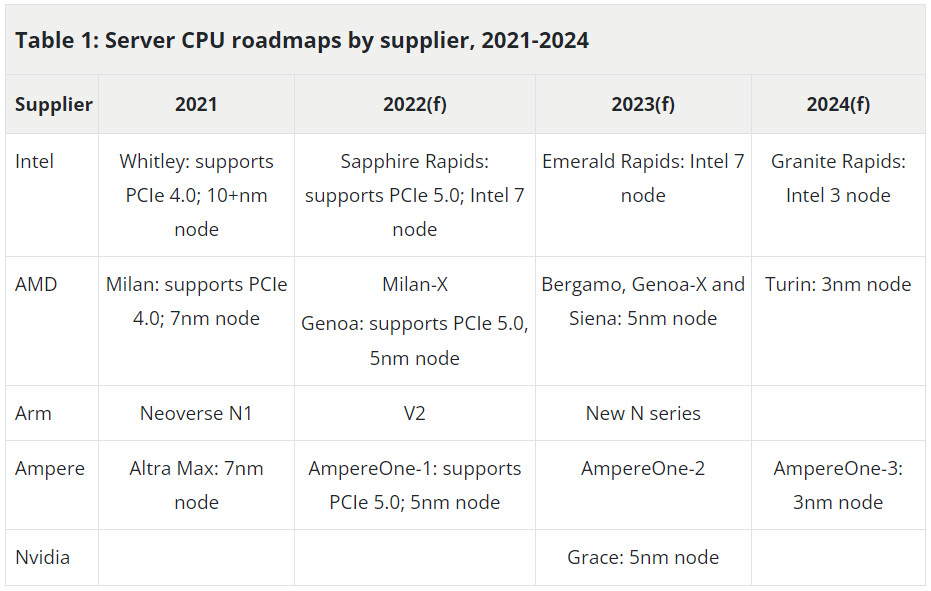
News Posts matching #chip

Return to Keyword Browsing

MediaTek Announces Commitment to Open New Semiconductor Design Center at Purdue University in Indiana

Today, leading global fabless chipmaker MediaTek Inc., [joined by Indiana Governor Eric J. Holcomb, Deputy Secretary of Commerce Don Graves, Indiana Secretary of Commerce Bradley B. Chambers, and Purdue College of Engineering's Dr. Mung Chiang] announced their commitment to accept a state transition assistance package from the Indiana Economic Development Commission (IEDC) to support its very first Midwest semiconductor chip design center in West Lafayette, Indiana. MediaTek also shared its intention to create a new research partnership with Purdue to collaborate on engineering talent development and new research on next-generation computing and communications chip design. The news was shared with senior leaders, other international investors and policymakers assembled in National Harbor, Maryland for the 2022 SelectUSA Investment Summit.

This novel partnership in Indiana represents a new U.S. growth model for MediaTek USA; outside the traditional centers of gravity for chip design. "We believe strongly that being in Indiana means we'll have access to some of the best engineering talent in the world," said Dr. Kou-Hung Lawrence Loh, Corporate Senior Vice President of MediaTek Inc. and President of MediaTek USA, Inc. "Not just at Purdue, but West Lafayette is only four hours away from nearly a dozen of the top engineering schools in the country. In the post pandemic world, top candidates tell us they want to be closer to home, near family and they want to have a real house and great schools. Indiana offers all that and more."

Intel Labs Announces Integrated Photonics Research Advancement

Intel Labs announces a significant advancement in its integrated photonics research - the next frontier in increasing communication bandwidth between compute silicon in data centers and across networks. The latest research features industry-leading advancements in multiwavelength integrated optics, including the demonstration of an eight-wavelength distributed feedback (DFB) laser array that is fully integrated on a silicon wafer and delivers excellent output power uniformity of +/- 0.25 decibel (dB) and wavelength spacing uniformity of ±6.5% that exceed industry specifications.

"This new research demonstrates that it's possible to achieve well-matched output power with uniform and densely spaced wavelengths. Most importantly, this can be done using existing manufacturing and process controls in Intel's fabs, thereby ensuring a clear path to volume production of the next-generation co-packaged optics and optical compute interconnect at scale." -Haisheng Rong, senior principal engineer at Intel Labs

Iceotope collaborates with Intel and HPE to accelerate sustainability and cut power for Edge and Data Center compute requirements by up to 30 Percent

Iceotope, the global leader in Precision Immersion Cooling, has announced that its chassis-level cooling system is being demonstrated in the Intel Booth at HPE Discover 2022, the prestigious "Edge-to-cloud Conference". Ku:l Data Center is the product of a close collaboration between Iceotope, Intel and HPE and promises a faster path to net zero operations by reducing edge and data center energy use by nearly a third. Once the sole preserve of arcane, high performance computing applications, liquid cooling is increasingly seen as essential technology for reliable and efficient operations of any IT load in any location. There is a pressing concern about sustainability impacts as distributed edge computing environments proliferate to meet the demand for data processing nearer the point of use, as well as growing facility power and cooling consumption driven by AI augmentation and hotter chips.

Working together with Intel and HPE, Iceotope benchmarked the power consumption of a sample IT installation being cooled respectively using air and precision immersion liquid cooling. The results show a substantial advantage in favour of liquid cooling, reducing overall power use across IT and cooling infrastructure.

AMD Instinct MI300 APU to Power El Capitan Exascale Supercomputer

The Exascale supercomputing race is now well underway, as the US-based Frontier supercomputer got delivered, and now we wait to see the remaining systems join the race. Today, during 79th HPC User Forum at Oak Ridge National Laboratory (ORNL), Terri Quinn at Lawrence Livermore National Laboratory (LLNL) delivered a few insights into what El Capitan exascale machine will look like. And it seems like the new powerhouse will be based on AMD's Instinct MI300 APU. LLNL targets peak performance of over two exaFLOPs and a sustained performance of more than one exaFLOP, under 40 megawatts of power. This should require a very dense and efficient computing solution, just like the MI300 APU is.

As a reminder, the AMD Instinct MI300 is an APU that combines Zen 4 x86-64 CPU cores, CDNA3 compute-oriented graphics, large cache structures, and HBM memory used as DRAM on a single package. This is achieved using a multi-chip module design with 2.5D and 3D chiplet integration using Infinity architecture. The system will essentially utilize thousands of these APUs to become one large Linux cluster. It is slated for installation in 2023, with an operating lifespan from 2024 to 2030.

Off-season Offsets Wafer Pricing Increase, 1Q22 Foundry Output Value Up 8.2% QoQ, Says TrendForce

According to TrendForce research, although demand for consumer electronics remains weak, structural growth demand in the semiconductor industry including for servers, high-performance computing, automotive, and industrial equipment has not flagged, becoming a key driver for medium and long term foundry growth. At the same time, due to robust wafer production at higher pricing in 1Q22, quarterly output value hit a new high for the 11th consecutive quarter, reaching US$31.96 billion, 8.2% QoQ, marginally less than the previous quarter. In terms of ranking, the biggest change is Nexchip surpassed Tower at the ninth position.

TSMC's across the board wafer hikes in 4Q21 on batches primarily produced in 1Q22 coupled with sustained strong demand for high-performance computing and better foreign currency exchange rates pushed TSMC's 1Q22 revenue to $17.53 billion, up 11.3% QoQ. Quarterly revenue growth by node was generally around 10% and the 7/6 nm and 16/12 nm processes posted the highest growth rate due to small expansions in production. The only instance of revenue decline came at the 5/4 nm process due to Apple's iPhone 13 entering the off season for production stocking.

NVIDIA RTX 40 Series Could Reach 800 Watts on Desktop, 175 Watt for Mobile/Laptop

Rumors of NVIDIA's upcoming Ada Lovelace graphics cards keep appearing. With every new update, it seems like the total power consumption is getting bigger, and today we are getting information about different SKUs, including mobile and desktop variants. According to a well-known leaker, kopite7kimi, we have information about the power limits of the upcoming GPUs. The new RTX 40 series GPUs will feature a few initial SKUs: AD102, AD103, AD104, and AD106. Every SKU, except the top AD102, will be available as well. The first in line, AD102, is the most power-hungry SKU with a maximum power limit rating of 800 Watts. This will require multiple power connectors and a very beefy cooling solution to keep it running.

Going down the stack, we have an AD103 SKU limited to 450 Watts on desktop and 175 Watts on mobile. The AD104 chip is limited to 400 Watts on desktop, while the mobile version is still 175 Watts. Additionally, the AD106 SKU is limited to 260 Watts on desktop and 140 Watts on mobile.

GlobalFoundries and STMicroelectronics Considering a New Fab in France

Recent news suggests that TSMC isn't too interested in setting up a fab in Europe, but it appears there are other interested parties that are now courting the EU, namely a potential joint venture between GlobalFoundries and STMicroelectronics. The two companies are hoping to get a slice of the same cake as Intel, namely the European Chips Act, to help subsidise the cost of the proposed fab. Although GlobalFoundries are headquartered in New York and STMicroelectronics in Geneva, the latter being a French-Italian conglomerate, the planned location for the new fab will be somewhere in France.

It's highly unlikely that this will be a cutting edge or even a leading edge fab, as neither company is in the business of producing products in those market segments. ST makes a wide range of chips from MCUs and other types of microprocessors, to specialised memory products, a wide range of sensors, MEMS based devices and all kinds of electronics for electrical vehicles, as well as highly specialised components for the space industry. GloFo obviously stepped off the competitive foundry ladder some years ago and have been focusing on specialised processes and nodes since then, such as FD-SOI, a technology, something the two companies announced a joint partnership around earlier this year. As such, it's likely that this potential fab will focus on making parts needed for the automotive industry in Europe, among other things. There's still a long way to go and neither company has made any kind of official statement about the potential partnership as yet.

Japan and the US Joins Forces to Produce 2 nm Chips in Japan by 2025

Based on a report by the Nikkei, Japan and the US have joined forces to speed up the development of semiconductor production at 2 nm nodes in Japan by 2025. It's not exactly clear how this is going to happen, but the two nations are said to have signed a bilateral chip technology partnership. The heavy lifting is said to be done by private companies from both nations, but in terms of research and actual chip production. Part of the reason for the move, is that Japan wants to be able to manufacture cutting edge ICs domestically for next-generation chips.

The research is said to be kicking off as soon as this summer, although no decisions have been made with regards to the manufacturing structure, with the Nikkei suggesting two alternatives, based on information from the Japanese Ministry of Economy. There will either be a joint partnership between Japanese and US businesses, or it could be a wholly Japanese owned setup. It appears that one major reason for this project is the production of ICs for the Japanese defence industry, as advanced electronics are needed in a lot of related products, ranging from fighter jets and missiles, to radar systems and communication systems. However, the article also suggests that the 2 nm node is suitable for everything from components for quantum computers to smartphones. Japan already makes advanced silicon wafers and many other parts and components used in semiconductor manufacturing, but the nation has fallen behind in the actual manufacturing of leading edge semiconductors over the past few years.

AMD set to Open Manufacturing Plant in Malaysia in Early 2023

AMD's Malaysian joint venture, TF-AMD Microelectronics is in the middle of the construction of a US$452 million manufacturing plant on the island of Penang off the west coast of Malaysia. The facility itself is said to cover 139,000 square metres and is said to create some 3,000 jobs related to advanced semiconductor engineering. The new plant will bring TF-AMD's total manufacturing space in Penang to 210,000 square metres, as the company already has a prior facility on the island.

The plant will allow AMD to expand the chip packaging side of its business, something that is going to be key for many of its future products, considering AMD appears to be focusing on manufacturing a wider range of chips that are made up from multiple chiplets. The TF in the name stands for TongFu, which is a Chinese IC assembly and testing company that AMD has partnered up with in Malaysia. The current plant does everything from wafer sorting to wafer level chip scale packaging to final testing and AMD chips made in Malaysia would have been assembled here.

Apple M1 Chips Affected by Unpatchable "PACMAN" Exploit

Apple M1 chips are a part of the Apple Silicon family that represents a new transition to Arm-based cores with new power and performance targets for Apple devices. A portion of building a processor is designing its security enclave, and today we have evidence that M1 processors got a new vulnerability. The PACMAN is a hardware attack that can bypass Pointer Authentication (PAC) on M1 processors. Security researchers took an existing concept of Spectre and its application in the x86 realm and now applied it to the Arm-based Apple silicon. PACMAN exploits a current software bug to perform pointer authentication bypass, which may lead to arbitrary code execution.

The vulnerability is a hardware/software co-design that exploits microarchitectural construction to execute arbitrary codes. PACMAN creates a PAC Oracle to check if a specific pointer matches its authentication. It must never crash if an incorrect guess is supplied and the attack brute-forces all the possible PAC values using the PAC Oracle. To suppress crashes, PAC Oracles are delivered speculatively. And to learn if the PAC value was correct, researchers used uArch side channeling. In the CPU resides translation lookaside buffers (TLBs), where PACMAN tries to load the pointer speculatively and verify success using the prime+probe technique. TLBs are filled with minimal addresses required to supply a particular TLB section. If any address is evicted from the TLB, it is likely a load success, and the bug can take over with a falsely authenticated memory address.
Apple M1 PACMAN Attack

TSMC Forecasts 30 Percent Increase in Sales for 2022

In 2021 TSMC saw an increase in sales of 24.9 percent in monetary value, but for 2022, the company is expecting this figure to reach somewhere around the 30 percent mark. For this quarter alone, TSMC is expecting a revenue of somewhere between US$17.6 to US$18.2 billion, with a gross margin ending up as high as 58 percent. Despite the positive outlook, TSMC hasn't been doing well on the Taiwanese stock exchange this year, as the company has lost more than a tenth of its value in 2022.

That said, TSMC is pressing forward and will still be spending in excess of US$40 billion in 2023 to expand its production capacity, following the US$40 to US$44 billion it will invest this year. The company isn't overly concerned about inflation at this point in time either, saying it doesn't have a direct impact on the semiconductor industry. TSMC is seeing a slowdown in the consumer chip space, but it's seeing an uptick in business when it comes to EV related ICs. TSMC's production lines are at full utilisation for at least the rest of 2022, but most likely long into 2023.

World's Top Ten IC Design Company Revenue Reached US$39.43 billion in 1Q22, Marvell Growth Rate Tops List, Says TrendForce

According to the latest TrendForce statistics, the top ten IC designers worldwide posted a combined revenue of US$39.43 billion in 1Q22, or 44% growth YoY. Qualcomm, NVIDIA, Broadcom ranked in the top three. After the acquisition of Xilinx, AMD surpassed MediaTek in the fourth position. In addition, according to TrendForce tracking of IC design industry trends, revenue generated by Will Semiconductor and Cirrus Logic was enough to be included in the top ten for the first time.

Benefiting from growth performance in handsets and RF front-end divisions in addition to its IoT and automotive divisions in 1Q22, Qualcomm's quarterly revenue reached US$9.55 billion, or 52% growth YoY, ranking number one in the world. The expanded application of GPUs in data centers boosted this portion of NVIDIA's revenue to 45.4%, surpassing the 45% accounted for by its gaming business, combining for a total revenue of US$7.9 billion, or 53% growth YoY. Broadcom's revenue from semiconductor solutions is substantial, including network chips, broadband communication chips, and storage and bridging chips. Its business has maintained stable sales performance, with revenue reaching US$6.11 billion, or 26% growth YoY. After the addition of Xilinx, AMD's revenue reached US$5.89 billion, or 71% growth YoY. However, even excluding Xilinx, due to strong sales in its enterprise, embedded and semi-customized divisions, AMD's own business revenue still hit an all-time high of US$5.33 billion.

AMD Selects Google Cloud to Provide Additional Scale for Chip Design Workloads

Google Cloud and AMD today announced a technology partnership in which AMD will run electronic design automation (EDA) for its chip-design workloads on Google Cloud, further extending the on-premises capabilities of AMD data centers. AMD will also leverage Google Cloud's global networking, storage, artificial intelligence, and machine learning capabilities to further improve upon its hybrid and multicloud strategy for these EDA workloads.

Scale, elasticity, and efficient utilization of resources play critical roles in chip design, particularly given that the demand for compute processing grows with each node advancement. To remain flexible and scale easily, AMD will add Google Cloud's newest compute-optimized C2D VM instance, powered by 3rd Gen AMD EPYC processors, to its suite of resources focused on EDA workloads. By leveraging Google Cloud, AMD anticipates being able to run more designs in parallel, giving the team more flexibility to manage short-term compute demands, without reducing allocation on long-term projects.

Phison Announces Successful Deployment of the World's First PCI-SIG Certified PCIe 5.0 Redriver IC PS7101

Phison Electronics Corp., a leading provider of NAND controller and NAND storage solutions integration services, announced today that it is successfully deploying the world's first PCIe 5.0 Redriver IC PS7101 certified by the PCI-SIG Association to help solve the compatibility problems of high-speed signal transmission between CPU (Central Processing Unit) and peripheral devices (such as SSD and graphics card, etc.). In the generation of PCIe 5.0 high-speed transmission, Redriver ICs will be required in devices such as desktop computers, servers, industrial computers, cables, and notebook computers. Depending on the degree of signal attenuation and the number of compensation channels, each system device will require 2 to 16 Redriver ICs. According to market research agencies, high-speed transmission signal enhancement ICs (including Redriver and Retimer ICs) will reach a market size of 50 million per year in 2025.

With the vigorous development of massive data, artificial intelligence, and cloud computing, demand for high-speed data transmission continues to rise. The CPU is the core of high-speed signal transmission. Under the leadership of CPU chip suppliers such as Intel and AMD, the transmission interface of the system has ushered the PCIe 5.0 generation, and the single-lane transmission speed reaching 32 Gbps per second, which is twice that of the previous generation PCIe 4.0. However, in the high-speed transmission environment of PCIe 5.0, compatibility issues such as signal attenuation and noise effects on the motherboard have become common problems and challenges faced by all system integrators.

GrAI Matter Labs Unveils sparsity-native AI SoC

GrAI Matter Labs, a pioneer of brain-inspired ultra-low latency computing, announced today that it will be unveiling GrAI VIP, a full-stack AI system-on-chip platform, to partners and customers at GLOBAL INDUSTRIE, May 17th-20th, 2022. At GLOBAL INDUSTRIE, GML will demonstrate a live event-based, brain-inspired computing solution for purpose-built, efficient inference in a real-world application of robotics using the Life-Ready GrAI VIP chip. GrAI VIP is an industry-first near-sensor AI solution with 16-bit floating-point capability that achieves best-in-class performance with a low-power envelope. It opens up unparalleled applications that rely on understanding and transformations of signals produced by a multitude of sensors at the edge in Robotics, AR/VR, Smart Homes, Infotainment in automobiles and more.

"GrAI VIP is ready to deliver Life-Ready AI to industrial automation applications and revolutionize systems such as pick & place robots, cobots, and warehouse robots, as being demonstrated at the show," said Ingolf Held, CEO of GrAI Matter Labs. "GrAI Matter Labs has a pipeline of over $1 Million in pre-orders, and we are thrilled to enable our early-access partners and customers in industrial automation, consumer electronics, defence and more, with our GrAI VIP M.2 cards sampling today." "GML is targeting the $1 billion+ fast-growing market (20%+ per year) of endpoint AI with a unique approach backed by innovative technology," said Karl Freund, Founder and Principal Analyst at Cambrian-AI Research. "GML's 'Life-Ready' AI provides solutions that here-to-fore were simply impossible at such low footprint and power." AI application developers looking for high fidelity and low latency responses for their edge algorithms can now get early access to the GrAI VIP platform and drive game-changing products in industrial automation, consumer electronics, and more.

Samsung Foundry Considering up to 20 Percent Price Hikes

Earlier this week, news about TSMC increasing prices in 2023 made its way online and now Samsung Foundry is said to be discussing price hikes with its customers to make up for the increased costs in materials. TSMC already increased its prices by around 20 percent at the end of 2021 and now it looks like Samsung Foundry is set to follow suit with a similar price hike. Depending on the node, the company is said to be looking at increases of between 15 to 20 percent. The somewhat peculiar thing in the case of Samsung Foundry, is that the company is looking at asking for more money on older, legacy nodes, than it will for its cutting edge nodes.

The price increases are said to come into effect sometime in the second half of 2022, so more than six months after TSMC's price hike. The company is still in negotiation with some of its customers, while others have already come to an agreement with Samsung Foundries. The costs to produce chips are said to be increasing by 20 to 30 percent across the board, no matter if we're talking materials needed to produce integrated circuits, or building new factories, according to Bloomberg. Samsung Foundries have also managed to secure long-term orders for the next five years, with a combined value of around eight times that of previous year's revenue, according to its EVP, Kang Moon-soo. The company is hoping to overtake TSMC in the future and invested more than US$36 billion in 2021 alone to expand its foundry business with new fabs and EUV machines. The good news is that Samsung Foundry claims to be back on track when it comes to yield on its 4 nm node and mass production of its 3 nm node is said to start this quarter.

TSMC Said to be Planning Price Increases in 2023

The global inflation rises are no secret and more and more companies are looking to increase prices of their goods, so not entirely unsurprising, reports of TSMC planning price hikes in early 2023 are starting to appear. TSMC has supposedly already contacted its customers to notify them about the upcoming price increase, to give them as much time as possible to make any changes to their plans, if needed. The price increase will vary depending on the node in question, but is reported to be somewhere between five and eight percent according to the Nikkei.

Part of the increase is also related to TSMC's rapid expansion that's going on at the moment, since the company is going to need to invest a lot more capital when it comes to building the advanced fabs that its customers are relying on. TSMC is expected to invest some US$40-44 billion this year alone on fabs and new equipment. This is a fairly small price increase compared to the big increase TSMC implemented in August 2021, where some nodes saw price hikes of up to 20 percent. That said, TSMC isn't alone in increasing their pricing, as UMC and SMIC have also increased their prices several times since last year. Nikkei claims that UMC and SMIC are charging more than TSMC on some nodes. However, in the past, TSMC used to offer discounts to its clients on a quarterly basis once a chip had gone into mass production and everything progressed smoothly, but TSMC discontinued this discount scheme last year. As such, it looks like cheaper chip costs aren't to be expected any time soon.

Montage Technology Starts Producing 2nd-Gen DDR5 RCDs

Montage Technology, a leading data processing and interconnect IC design company, today announced it is now producing its 5600 MT/s 2nd-generation DDR5 RCD (RCD02) chip to support memory module vendors to enable the DDR5-5600 ecosystem. The new device is targeted for demanding applications such as next-generation servers, edge computing, and AI. The RCD02 is compliant with the latest JEDEC DDR5RCD02 specification. Compared with the 1st-generation RCD (RCD01), the RCD02 boosts DDR5 data rate by 16.67%. The RCD02 chip adopts dual-channel memory architecture, supports 1.1 V VDD and 1.0 V VDDIO voltages and several power saving modes, thus enabling a great reduction in power consumption.

In addition to providing industry-leading performance, power efficiency and reliability at the device level, Montage's DDR5 RCD02 solution supports CA, CS and DFE training modes, dual frequency, as well as other advanced features to facilitate the higher speed for the next generation DDR5 platform.
"An insatiable demand for bandwidth in everything from high-performance computing to AI training, gaming, is fueling the development of the next-generation memory," said Montage Technology's President, Stephen Tai. "Montage is delighted to be the first in the industry to successfully produce the DDR5 RCD02 chip to help meet the ever-increasing demand for memory bandwidth."

ISMC to Build US$3 Billion Chip Foundry in India

International semiconductor consortium or ISMC is a new joint venture between Abu Dhabi-based Next Orbit Ventures and Israeli Tower Semiconductor that is getting ready to invest big. The consortium is said to be looking at investing no less than US$3 billion in a chip foundry based in Karnataka, India. Maybe the most interesting part here is that Tower Semiconductor is set to be acquired by Intel, assuming the deal passes all regulatory reviews. This means that Intel could be replacing Tower Semiconductor in the consortium before the new fab has been finished.

Not much information is available about ISMC, but the planned chip plant would be one of the first foundries in India, as well as the largest foundry in the nation. So far ISMC has only signed a memorandum of Understanding with the government of Karnataka, so things could still change. However, the US$10 billion incentive by the central Indian government might be part of the reason behind the decision. Tower Semiconductor specialises in various speciality process technologies, such as SiGe, BiCMOS and SOI and manufacturer mixed-signal and RFCMOS chips, as well as CMOS based image sensors, power management chips and various types of non-volatile memory and some MEMS products for its customers. The new fab is expected to bring 1,500 direct and some 10,000 indirect jobs to the region.

Intel CEO Expects Chip Shortage to Last Until 2024

In an interview with CNBC's TechCheck, Intel CEO Pat Gelsinger said he expected the chip shortage to continue to drag on, at least until 2024. Unfortunately he didn't go into too much detail as to why, beyond there being an equipment shortage, which in turn will slow down the speed at which new fabs can be put online. In other words, Intel is pointing fingers at ASML and other companies that manufacture the various types of equipment that is needed to manufacture semiconductors.

Intel is the first company to have publicly said that the semiconductor shortage will continue longer than initially expected, where most companies expected things to ease off towards the end of this year, or at least sometime in 2023. The shortage isn't likely to affect Intel when it comes to products the company manufactures in-house, but if the shortage continues into the foreseeable future, it might have a bigger knock-on effect when it comes to the wide ecosystem that Intel is reliant on, such as motherboards. The other concern is obviously Intel's products that are being manufactured by TSMC, where the company is likely to see increased competition when it comes to getting access to enough capacity at certain production nodes.

TSMC Founder Says Growing Domestic US Chip Production is Wasteful and Expensive

According to an article over on The Register, the TSMC founder, Morris Chang, isn't overly impressed by US efforts to grow its domestic chip production. In a podcast hosted by the Brookings Institution, Morris Chang said that the US' attempt to grow its domestic chip production will be "a wasteful, expensive exercise in futility." The reason behind his comment is that he believes the US is lacking the talent to work in the fabs, or possibly the willingness to work triple-shift to keep the fabs running 24/7, unlike the Taiwanese. Furthermore, he states that the US can't compete in terms of cost, as he claims it's 50 percent more expensive to manufacture chips in the US compared to Taiwan.

It should be pointed out that Morris Chang is no longer involved with the day to day operations at TSMC and the above are just his opinion. When questioned about why TSMC is building a fab in Arizona, Chang said that TSMC decided to do it because they were urged to do so by the US government. He also believes that despite government subsidies, the US is unlikely to become self-sufficient when it comes to semiconductors, especially as the cost per chip will be much higher, which will make it hard to compete internationally. However, he does mention that if the PRC decided to start a war with Taiwan, then the bet is likely to pay off for the US, but there are obviously other problems that such a situation would bring as well. Chang also praises US chip design talent and says that Taiwan has very little talent in comparison and that TSMC has none. However, the latter doesn't seem to be entirely true, based on the fact that TSMC is helping its customers to optimise their designs for the various production nodes at TSMC. For those interested, the podcast can be found below.

Intel Sapphire Rapids 56-Core ES Processor Boosts to 3.3 GHz at 420 Watts

Intel is slowly transitioning its data center customers to a new processor generation called Sapphire Rapids. Today, thanks to the hardware leaker Yuuki_ans we have more profound insights into the top-end 56-core Sapphire Rapids processor and its power settings. According to the leak, we have information on either Xeon Platinum 8476 or Platinum 8480 designs that are equipped with 56 cores and 112 threads. This model was running at the base frequency of 1.9 GHz and a boost frequency of 3.3 GHz. Single-core can boost to 3.7 GHz if the report is giving a correct reading. Remember that this is only an engineering sample, so the final target speeds could differ. It carries 112 MB of L2 and 105 MB of L3 cache, and this sample was running with 1 TB of DDR5 memory with CL40-39-38-76 timings.

Perhaps the most exciting finding is the power configuration of this SKU. Intel has enabled this CPU to consume 350 Watts in PL1 rating, with up to 420 Watts in PL2 performance mode. The enforced BIOS power limit rating is set at an astonishing 764 Watts, which could happen with AVX-512 enabled. Final TDP ratings are yet to be disclosed; however, these Sapphire Rapids processors are shaping to be relatively power-hungry chips.

Ancillary Semiconductors Require in Excess of Six Months Lead Time

Based on a report by Susquehanna, the lead time for what can be called ancillary semiconductors, i.e. the kind that are paired up with processor, SoCs and GPUs, now have a lead time of over six months. This is based on data from the distribution channel and as such, it's unlikely to affect large companies that have long-term contracts with their suppliers. However, smaller companies, or semiconductor manufacturers that solely rely on the distribution channel for sales of the parts, are not in a good place right now. Obviously this doesn't affect everything equally and many parts are also in stock with the big distributors, but sometimes at inflated prices compared to a couple of years ago.

Susquehanna is pointing towards several reasons for the increase in lead times, although the big ones include the Russia's war on Ukraine, an earthquake in Japan (on the 16th of March) as well as the more recent lockdowns in several cities in the PRC which are key to the production of everything from semiconductors to finished consumer goods. At the latter half of 2020, the lead time was less than 14 weeks, but has since then increased to almost 27 weeks and it looks like it's likely to continue to increase for the time being. The worst hit components are said to be analogue chips, so things like signal amplifiers, power control oscillators and the like, which had the lead times increased by 18 over the space of a month. The report says that Broadcom has increased its shipping times by as much as 30 weeks and its backlog of orders just keeps growing. This is quite surprising, as earlier reports mentioned that the WiFi makers were reasonably unaffected by the increase in lead times, but Broadcom does make a wealth of other products too, so this could be unrelated. On a more positive note, it seems like the lead time for passive components has improved by a couple of days, with an average lead time of 25 weeks.

TSMC First Quarter 2022 Financials Show 45.1% Increase in Revenues

A new quarter and another forecast shattering revenue report from TSMC, as the company beat analysts' forecasts by over US$658 million, with a total revenue for the quarter of US$17.6 billion and a net income of almost US$7.26 billion. That's an increase in net income of 45.1 percent or 35.5 percent in sales. Although the monetary figures might be interesting to some, far more interesting details were also shared, such as production updates about future nodes. As a followup on yesterday's news post about 3 nanometer nodes, the N3 node is officially on track for mass production in the second half of this year. TSMC says that customer engagement is stronger than at the start of its N7 and N7 nodes, with HPC and smartphone chip makers lining up to get onboard. The N3E node is, as reported yesterday, expected to enter mass production in the second half of 2023, or a year after N3. Finally, the N2 node is expected in 2025 and won't adhere to TSMC's two year process technology cadence.

Breaking down the revenue by nodes, N7 has taken back the lead over N5, as N7 accounted for 30 percent of TSMC's Q1 revenues up from 27 percent last quarter, but down from 35 percent in the previous year. N5 sits at 20 percent, which is down from 23 percent in the previous quarter, but up from 14 percent a year ago. The 16 and 28 nm nodes still hold on to 25 percent of TSMC's revenue, which is the same as a year ago and up slightly from the previous quarter. Remaining nodes are unchanged from last quarter.

Polyn Technology Delivers NASP Test Chip for Tiny AI

Polyn Technology announced today that its first Neuromorphic Analog Signal Processor (NASP) chip is packaged and evaluated, demonstrating proof of the technology's brain-mimicking architecture. It is the first Tiny AI true analog design to be used next to sensors. Polyn Technology is an innovative provider of ultra-low-power-performance NASP technology and a producer of unique Tiny AI chips and their associated IP. "This achievement validates the intensive work of our multinational team," said Aleksandr Timofeev, CEO and founder of Polyn Technology. "Our chip represents the most advanced technology bridging analog computations and the digital core. It is designed with neuroscience in mind, replicating pre-processing the primary cortical area of the human brain does at the periphery before learning at the center."

The NASP chip enables full data processing disaggregation between the sensor node and the cloud; it truly embodies the Tiny AI concept. The NASP test chip contains several neural networks. The chip is implemented in 55 nm CMOS technology. Its design proves the NASP "neuron" model as well as the scalability of the technology and efficiency of the chip design automation tools developed by Polyn. "Our first chip is created from trained neural networks by NASP Compiler and synthesis tools that generated Netlist and the silicon engineering files from the software math model simulation. We will continue to refine our technology for creation of new generation chips," said Yaakov Milstain, COO of Polyn. Polyn anticipates the chip will be available to customers in the first quarter of 2023 as its first wearables product, with a fusion of PPG and IMU sensors for the most accurate heart rate measurement along with recognition and tracking of human activity.
Return to Keyword Browsing
Jul 16th, 2024 00:33 EDT change timezone

New Forum Posts

Popular Reviews

Controversial News Posts