News Posts matching #chip

Return to Keyword Browsing

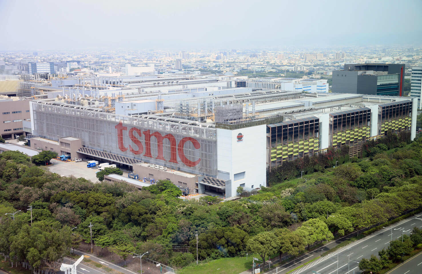
TSMC and Partners to Invest $11 Billion into German-based Factory

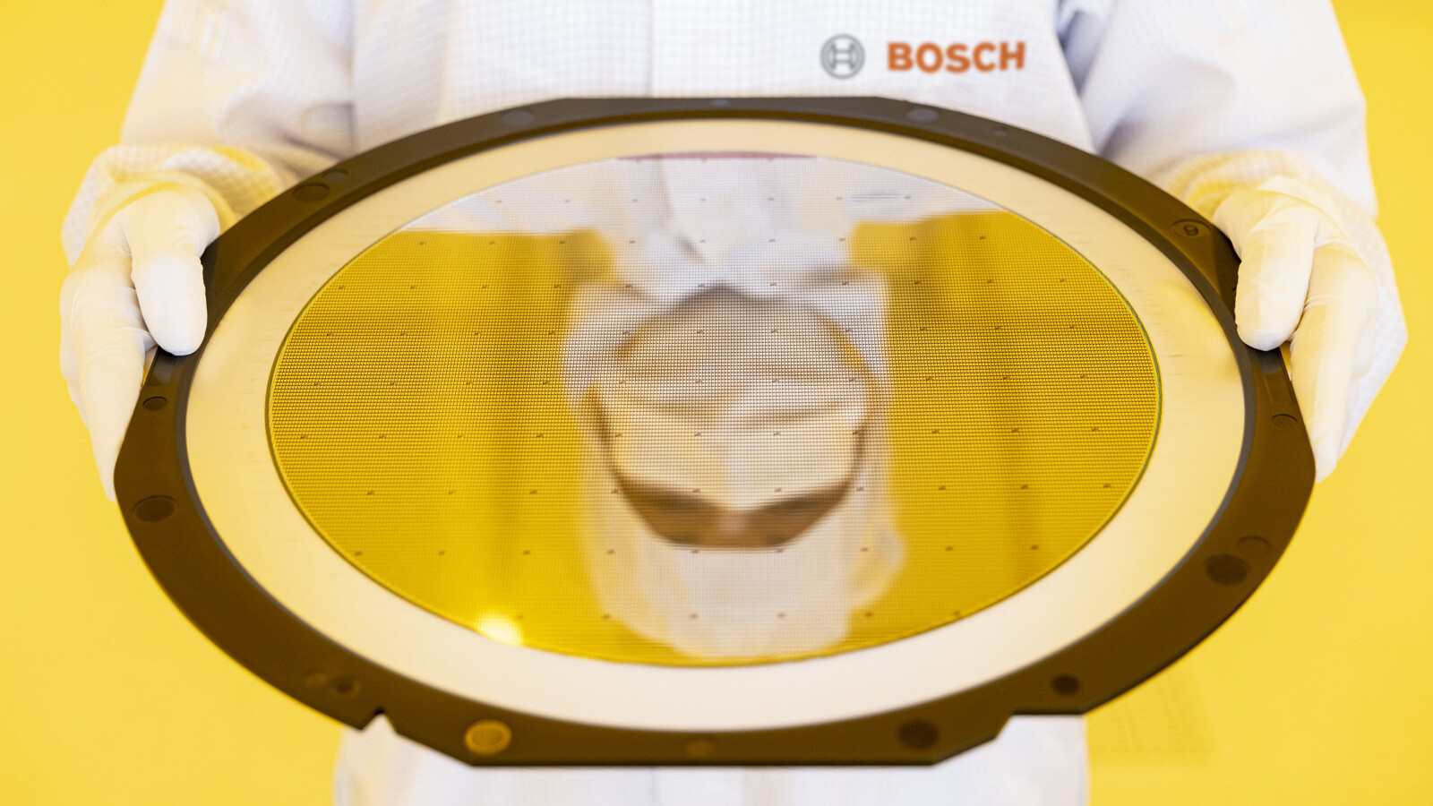
TSMC, a Taiwanese semiconductor giant, is reportedly talking to its partners to develop an $11 billion (€10 billion) factory in Germany with the help of a few European partners. Currently assessing the plant location for Saxony in Germany, the fab wouldn't only be exclusively made by TSMC but will bring in NXP, Bosch, and Infineon that, will create a budget of around 7 billion Euros, including state subsidies, while the total budget is leaning closer to 10 billion Euros in total. However, it is essential to note that TSMC is still assessing the possibility of a Europe-based plant altogether.

Asking for as much as 40% of the total investment to be European-backed subsidies, TSMC wants to create a European facility that will be focused on a growing sector--automotive. If approved in August, the TSMC plant will become the company's first European facility and will first focus on manufacturing 28 nm chips. As one of the first significant EU Chips Act €43 billion investment, it will heavily boost European semiconductor manufacturing.

Microsoft Said to be Designing its own Arm SoC to Compete with Apple Silicon

According to Tom's Hardware, Microsoft is busy hiring engineers to help the company design its own Arm based SoC for Windows 12. Based on job listings, Microsoft is adding people to its "Silicon team," which is currently involved in designing products for Microsoft's Azure, Xbox Surface and HoloLens products. That said, the specific job listings mentioned by Tom's Hardware mentions "optimizing Windows 12 for Silicon-ARM architecture" suggesting we're looking at a custom Arm SoC, with others mentioning "internally developed silicon components" and "building complex, state-of-the-art SOCs using leading silicon technology nodes and will collaborate closely with internal customers and partners."

That said, Microsoft is currently working with Qualcomm and the Microsoft SQ3 found in the Surface Pro 9 is the latest result of that partnership. This brings the question if Microsoft has decided to make its own chip to compete with the Apple M-series of silicon, or if Microsoft is simply looking at working closer with Qualcomm by hiring inhouse talent that can help tweak the Qualcomm silicon to better suit its needs. With Windows 12 scheduled for a 2024 release, it looks like we'll have to wait a while longer to find out what Microsoft is cooking up, but regardless of what it is, it looks like Windows on Arm isn't going anywhere.

Qualcomm Said to be Considering Samsung for 3 nm Snapdragon 8 Gen 4 chips

It appears it's not only AMD that is eyeing a move to Samsung, when it comes to fabricating upcoming chips, as reports are now suggesting that Qualcomm is considering a second attempt at making flagship mobile SoCs at Samsung's foundry. However, in this case, we're talking 3 nm chips in the shape of the Snapdragon 8 Gen 4, which is expected to launch in devices sometime in 2024. This is said to be Qualcomm's first chip based on cores built by Nuvia, a company that Qualcomm acquired in 2021.

That said, Qualcomm will apparently not rely on Samsung alone, but will also be making the Snapdragon 8 Gen 4 at TSMC. This might be because of past experience with Samsung, but the report out of Taiwan, suggests that the chips made by Samsung's foundry business will be used in Samsung branded phones, whereas the TSMC made chips might end up in devices by Qualcomm's other customers. It could also be a bet for Qualcomm to try and get better pricing by both foundries or a means of hedging their bets, to see which foundry produces the better chips. Then there's the situation between the PRC and the ROC, which could potentially put Qualcomm in a situation where it has no chips, so going with Samsung could be a means of covering for all potential risk scenarios.

MIT Researchers Grow Transistors on Top of Silicon Wafers

MIT researchers have developed a groundbreaking technology that allows for the growth of 2D transition metal dichalcogenide (TMD) materials directly on fully fabricated silicon chips, enabling denser integrations. Conventional methods require temperatures of about 600°C, which can damage silicon transistors and circuits as they break down above 400°C. The MIT team overcame this challenge by creating a low-temperature growth process that preserves the chip's integrity, allowing 2D semiconductor transistors to be directly integrated on top of standard silicon circuits. The new approach grows a smooth, highly uniform layer across an entire 8-inch wafer, unlike previous methods that involved growing 2D materials elsewhere before transferring them to a chip or wafer. This process often led to imperfections that negatively impacted device and chip performance.

Additionally, the novel technology can grow a uniform layer of TMD material in less than an hour over 8-inch wafers, a significant improvement from previous methods that required over a day for a single layer. The enhanced speed and uniformity of this technology make it suitable for commercial applications, where 8-inch or larger wafers are essential. The researchers focused on molybdenum disulfide, a flexible, transparent 2D material with powerful electronic and photonic properties ideal for semiconductor transistors. They designed a new furnace for the metal-organic chemical vapor deposition process, which has separate low and high-temperature regions. The silicon wafer is placed in the low-temperature region while vaporized molybdenum and sulfur precursors flow into the furnace. Molybdenum remains in the low-temperature region, while the sulfur precursor decomposes in the high-temperature region before flowing back into the low-temperature region to grow molybdenum disulfide on the wafer surface.

Bosch Plans to Acquire U.S. Chipmaker TSI Semiconductors

Bosch is expanding its semiconductor business with silicon carbide chips. The technology company plans to acquire assets of the U.S. chipmaker TSI Semiconductors, based in Roseville, California. With a workforce of 250, the company is a foundry for application-specific integrated circuits, or ASICs. Currently, it mainly develops and produces large volumes of chips on 200-millimeter silicon wafers for applications in the mobility, telecommunications, energy, and life sciences industries. Over the next years, Bosch intends to invest more than 1.5 billion USD in the Roseville site and convert the TSI Semiconductors manufacturing facilities to state-of-the-art processes. Starting in 2026, the first chips will be produced on 200-millimeter wafers based on the innovative material silicon carbide (SiC).

In this way, Bosch is systematically reinforcing its semiconductor business, and will have significantly extended its global portfolio of SiC chips by the end of 2030. Above all, the global boom and ramp-up of electromobility are resulting in huge demand for such special semiconductors. The full scope of the planned investment will be heavily dependent on federal funding opportunities available via the CHIPS and Science Act as well as economic development opportunities within the State of California. Bosch and TSI Semiconductors have reached an agreement to not to disclose any financial details of the transaction, which is subject to regulatory approval.

SK Hynix Believes the Memory Chip Market Has Hit Rock Bottom

Yesterday SK Hynix reported its Q1 2023 results and to say that they were abysmal is being kind, as the company reported a 3.4 trillion won operating loss, or just over US$2.5 billion. That's no small hit to take for any company, especially when it's only the performance for a single quarter. However, SK Hynix is apparently trying to see its situation from a positive perspective and believes that the memory chip market will rebound in the second half of this year. The positive outlook isn't just based on what SK Hynix believes though, as various analysts and securities companies believe in an upswing in the second half of the year.

That said, Micron, one of SK Hynix main competitors, has a more drab outlook for the remainder of 2023 and is expecting a tough year ahead. SK Hynix is expecting production cuts by itself, Micron and Samsung to start to take effect sometime in the second quarter this year, which should see inventory drop to more normal levels for all three companies. SK Hynix is also expecting to see a higher demand for DDR5 DRAM later this year, especially in the mobile and server market space. Finally, SK Hynix is hoping that its customers will buy higher density memory products this year, replacing older, lower density solutions, be that DRAM or NAND flash related. SK Hynix is expecting to launch its Gen 5 10 nm DRAM and 238-layer NAND sometime next year, which the company is also hoping will bring more income to its coffers, but the company still has to make it through the rest of 2023 first.

TSMC Certifies Ansys Multiphysics Solutions for TSMC's N2 Silicon Process

Ansys and TSMC continue their long-standing technology collaboration to announce the certification of Ansys' power integrity software for TSMC's N2 process technology. The TSMC N2 process, which adopts nanosheet transistor structure, represents a major advancement in semiconductor technology with significant speed and power advantages for high performance computing (HPC), mobile chips, and 3D-IC chiplets. Both Ansys RedHawk-SC and Ansys Totem are certified for power integrity signoff on N2, including the effects of self-heat on long-term reliability of wires and transistors. This latest collaboration builds on the recent certification of the Ansys platform for TSMC's N4 and N3E FinFLEX processes.

"TSMC works closely with our Open Innovation Platform (OIP) ecosystem partners to help our mutual customers achieve the best design results with the full stack of design solutions on TSMC's most advanced N2 process," said Dan Kochpatcharin, head of the Design Infrastructure Management Division at TSMC. "Our latest collaboration with Ansys RedHawk-SC and Totem analysis tools allows our customers to benefit from the significant power and performance improvements of our N2 technology while ensuring predictively accurate power and thermal signoff for the long-term reliability of their designs."

Samsung Electronics Announces First Quarter 2023 Results, Profits Lowest in 14 Years

Samsung Electronics today reported financial results for the first quarter ended March 31, 2023. The Company posted KRW 63.75 trillion in consolidated revenue, a 10% decline from the previous quarter, as overall consumer spending slowed amid the uncertain global macroeconomic environment. Operating profit was KRW 0.64 trillion as the DS (Device Solutions) Division faced decreased demand, while profit in the DX (Device eXperience) Division increased.

The DS Division's profit declined from the previous quarter due to weak demand in the Memory Business, a decline in utilization rates in the Foundry Business and continued weak demand and inventory adjustments from customers. Samsung Display Corporation (SDC) saw earnings in the mobile panel business decline quarter-on-quarter amid a market contraction, while the large panel business slightly narrowed its losses. The DX Division's results improved on the back of strong sales of the premium Galaxy S23 series as well as an enhanced sales mix focusing on premium TVs.

Rapidus to Start Production of 2 nm Fab in Chitose, Gets Cash Injection from Japanese Government

Future Japanese chipmaker Rapidus has announced that their first fab will be located in Chitose, Hokkaido, located in northern Japan. The planned 2 nm fab will be one of the most advanced fabs in the world once it's ready and construction is said to be starting in September, thanks to approval by the related Japanese government agencies. So far, the Japanese government has approved 330 billion yen for Rapidus, with the most recent investment being 260 billion yen or the equivalent of US$1.94 billion.

However, the total investment into the 2 nm fab is expected to end up somewhere around 5 trillion yen (~US$37.5 billion) in total investments before the fab is ready for mass production. Rapidus is collaborating with IBM and has already sent a group of researchers to its Albany Nanotech facility in upstate New York, which is one of the world's most advanced semiconductor research facilities. At the same time, Japan is working on building a local talent pool of researchers and semiconductor plant workers, by spearheading specialised training for select university students from Japan's top universities. Time will tell if this gamble pays off for Japan, as it's going to be a huge investment before the new fab stands ready in early 2025.

NVIDIA Prepares H800 Adaptation of H100 GPU for the Chinese Market

NVIDIA's H100 accelerator is one of the most powerful solutions for powering AI workloads. And, of course, every company and government wants to use it to power its AI workload. However, in countries like China, shipment of US-made goods is challenging. With export regulations in place, NVIDIA had to get creative and make a specific version of its H100 GPU for the Chinese market, labeled the H800 model. Late last year, NVIDIA also created a China-specific version of the A100 model called A800, with the only difference being the chip-to-chip interconnect bandwidth being dropped from 600 GB/s to 400 GB/s.

This year's H800 SKU also features similar restrictions, and the company appears to have made similar sacrifices for shipping its chips to China. From the 600 GB/s bandwidth of the regular H100 PCIe model, the H800 is gutted to only 300 GB/s of bi-directional chip-to-chip interconnect bandwidth speed. While we have no data if the CUDA or Tensor core count has been adjusted, the sacrifice of bandwidth to comply with export regulations will have consequences. As the communication speed is reduced, training large models will increase the latency and slow the workload compared to the regular H100 chip. This is due to the massive data size that needs to travel from one chip to another. According to Reuters, an NVIDIA spokesperson declined to discuss other differences, stating that "our 800 series products are fully compliant with export control regulations."

Global Fab Equipment Spending on Track for 2024 Recovery After 2023 Slowdown

Global fab equipment spending for front-end facilities is expected to decrease 22% year-over-year (YoY) to US$76 billion in 2023 from a record high of US$98 billion in 2022 before rising 21% YoY to US$92 billion in 2024 to reclaim lost ground, SEMI announced today in its latest quarterly World Fab Forecast report. The 2023 decline will stem from weakening chip demand and higher inventory of consumer and mobile devices.

Next year's fab equipment spending recovery will be driven in part by the end of the semiconductor inventory correction in 2023 and strengthening demand for semiconductors in the high-performance computing (HPC) and automotive segments. "This quarter's SEMI World Fab Forecast update offers our first look ahead to 2024, highlighting the steady global expansion of fab capacity to support future semiconductor industry growth driven by the automotive and computing segments and a host of emerging applications," said Ajit Manocha, SEMI president and CEO. "The report points to a healthy 21% uptick in equipment investment next year."

Qualcomm Expands Connected Intelligent Edge Ecosystem Through Groundbreaking IoT and Robotics Products

Qualcomm Technologies, Inc. today announced the world's first integrated 5G IoT processors that are designed to support four major operating systems, in addition to two new robotics platforms, and an accelerator program for IoT ecosystem partners. These new innovations will empower manufacturers participating in the rapidly expanding world of devices at the connected intelligent edge.

The need for connected, intelligent, and autonomous devices is growing rapidly, and it is expected to hit $116 billion by 2030 according to Precedence Research. Businesses attempting to compete in this fast-moving economy need a reliable source of control and connectivity technology for their IoT and robotic devices. Qualcomm Technologies, which has shipped over 350 million dedicated IoT chipsets, is uniquely capable of providing manufacturers with the platforms needed to address this expanding segment.

South Korean Company Morumi is Developing a CPU with Infinite Parallel Processing Scaling

One of the biggest drawbacks of modern CPUs is that adding more cores doesn't equal more performance in a linear fashion. Parallelism in CPUs offer limited scaling for most applications and even none for some. A South Korean company called Morumi is now taking a stab at solving this problem and wants to develop a CPU that can offer more or less infinite processing scaling, as more cores are added. The company has been around since 2018 and focused on various telecommunications chips, but has now started the development on what it calls every one period parallel processor (EOPPP) technology.

EOPPP is said to distribute data to each of the cores in a CPU before the data is being processed, which is said to be done over a type of mesh network inside the CPU. This is said to allow for an almost unlimited amount of instructions to be handled at once, if the CPU has enough cores. Morumi already has an early 32-core prototype running on an FPGA and in certain tasks the company has seen a tenfold performance increase. It should be noted that this requires software specifically compiled for EOPPP and Moumi is set to release version 1.0 of its compiler later this year. It's still early days, but it'll be interesting to see how this technology develops, but if it's successfully developed, there's also a high chance of Morumi being acquired by someone much bigger that wants to integrate the technology into their own products.

Netherlands Government Sets Restrictions on Chip Exports, ASML Responds

Today the Dutch government has published more information on upcoming restrictions on export of semiconductor equipment. These new export controls focus on advanced chip manufacturing technology, including the most advanced deposition and immersion lithography tools. Due to these upcoming regulations, ASML will need to apply for export licenses for shipment of the most advanced immersion DUV systems.

It will take time for these controls to be translated into legislation and take effect. Based on today's announcement, our expectation of the Dutch government's licensing policy, and the current market situation, we do not expect these measures to have a material effect on our financial outlook that we have published for 2023 or for our longer-term scenarios as announced during our Investor Day in November last year.

Axelera AI and Advantech Are Teaming up to Bring the Inference Power of a Data Center to Edge Devices

Axelera AI, the provider of world's most powerful and advanced solutions for AI at the Edge today announces a strategic partnership with Advantech. Combining Advantech's expertise in the embedded and industrial PCs and Axelera AI's disruptive edge AI technology, together they will bring the inference power of a data center to edge devices, enabling customers to process data in real-time, reducing latency while increasing efficiency.

At Embedded World Axelera AI will show its new products, available in a range of industry-standard form factors varying from M.2 modules to vision ready systems. The products combine powerful processing performance with Metis AIPU technology and the easy-to-use Voyager SDK software stack, just at a fraction of the cost and power consumption of today's available solutions.

Hailo Introduces Hailo-15: The First AI-Centric Vision Processors for Next-Generation Intelligent Cameras

Hailo, the pioneering chipmaker of edge artificial intelligence (AI) processors, today announced its groundbreaking new Hailo-15 family of high-performance vision processors, designed for integration directly into intelligent cameras to deliver unprecedented video processing and analytics at the edge. With the launch of Hailo-15, the company is redefining the smart camera category by setting a new standard in computer vision and deep learning video processing, capable of delivering unprecedented AI performance in a wide range of applications for different industries.

With Hailo-15, smart city operators can more quickly detect and respond to incidents; manufacturers can increase productivity and machine uptime; retailers can protect supply chains and improve customer satisfaction; and transportation authorities can recognize everything from lost children, to accidents, to misplaced luggage. "Hailo-15 represents a significant step forward in making AI at the edge more scalable and affordable," stated Orr Danon, CEO of Hailo. "With this launch, we are leveraging our leadership in edge solutions, which are already deployed by hundreds of customers worldwide; the maturity of our AI technology; and our comprehensive software suite, to enable high performance AI in a camera form-factor."

Price War Looming for Mature Fab Nodes in Taiwan

The smaller foundries in Taiwan—at least compared to TSMC—UMC, PSMC and VIS to name the bigger players, but also other less well known foundries that produce chips on mature nodes, are getting ready for what looks like a price war. In all fairness, all of these companies have hiked their prices multiple times over the past couple of years, so it might just be a return to more normal pricing for these nodes that we're looking at. According to UDN media in Taiwan, the smaller foundries are offering discounts that range between 10 and 20 percent for new orders placed with them.

This is largely due to underutilised production lines for some nodes and the companies are trying to increase the utilisation rate of these nodes. The article mentions that the foundries with 8-inch wafer lines are those hardest hit, especially as they've produced more specialised ICs, such as fingerprint sensors, various driver ICs and power management ICs to mention a few. Some of these foundries are now running at 50 to 60 percent of their capacity, which doesn't bode well for the industry. On the other hand, 12-inch fabs aren't nearly as badly hit and might not offer as attractive discounts to potential customers. Another threat to the Taiwanese foundries is Samsung, which is reportedly also offering around a 10 percent discount on its mature nodes.

Ayar Labs Demonstrates Industry's First 4-Tbps Optical Solution, Paving Way for Next-Generation AI and Data Center Designs

Ayar Labs, a leader in the use of silicon photonics for chip-to-chip optical connectivity, today announced public demonstration of the industry's first 4 terabit-per-second (Tbps) bidirectional Wavelength Division Multiplexing (WDM) optical solution at the upcoming Optical Fiber Communication Conference (OFC) in San Diego on March 5-9, 2023. The company achieves this latest milestone as it works with leading high-volume manufacturing and supply partners including GlobalFoundries, Lumentum, Macom, Sivers Photonics and others to deliver the optical interconnects needed for data-intensive applications. Separately, the company was featured in an announcement with partner Quantifi Photonics on a CW-WDM-compliant test platform for its SuperNova light source, also at OFC.

In-package optical I/O uniquely changes the power and performance trajectories of system design by enabling compute, memory and network silicon to communicate with a fraction of the power and dramatically improved performance, latency and reach versus existing electrical I/O solutions. Delivered in a compact, co-packaged CMOS chiplet, optical I/O becomes foundational to next-generation AI, disaggregated data centers, dense 6G telecommunications systems, phased array sensory systems and more.

Biden-Harris Administration Launches First CHIPS for America Funding Opportunity

The Biden-Harris Administration through the U.S. Department of Commerce's National Institute of Standards and Technology today launched the first CHIPS for America funding opportunity for manufacturing incentives to restore U.S. leadership in semiconductor manufacturing, support good-paying jobs across the semiconductor supply chain, and advance U.S. economic and national security.

As part of the bipartisan CHIPS and Science Act, the Department of Commerce is overseeing $50 billion to revitalize the U.S. semiconductor industry, including $39 billion in semiconductor incentives. The first funding opportunity seeks applications for projects to construct, expand, or modernize commercial facilities for the production of leading-edge, current-generation, and mature-node semiconductors. This includes both front-end wafer fabrication and back-end packaging. The Department will also be releasing a funding opportunity for semiconductor materials and equipment facilities in the late spring, and one for research and development facilities in the fall.

Intel Accelerates 5G Leadership with New Products

For more than a decade, Intel and its partners have been on a mission to virtualize the world's networks, from the core to the RAN (radio access network) and out to the edge, moving them from fixed-function hardware onto programmable, software-defined platforms, making networks more agile while driving down their complexity and cost.

Now operators are looking to cross the next chasm in delivering cloud-native functionality for automating, managing and responding to an increasingly diverse mix of data and services, providing organizations with the intelligence needed at the edge of their operations. Today, Intel announced a range of products and solutions driving this transition and broad industry support from leading operators, original equipment manufacturers (OEMs) and independent software vendors (ISVs).

TSMC Said to be Planning Second Fab in Japan

The rumour mill has kicked into high gear this week about TSMC planning a second fab in Japan. The original source is the Nikkan Kogyo newspaper (via Reuters), based in Tokyo, although it's unclear where the actual fab would be located, if it's indeed even happening. According to the paper, the new fab would be focusing on 5 and 10 nanometer chips, but production isn't expected to start until sometime in the second half of this decade. This suggests that these would be mainstream nodes by then, which points to yet another fab for either the vehicle industry or something similar.

The fab is said to cost more than a trillion yen, or over US$7.4 billion to build. TSMC's CEO C.C. Wei was asked about the potential fab during TSMC's latest earnings call, but simply said that the company had nothing further to add. TSMC is of course busy building a fab in Japan on Kyushu island, but as it'll have a node capacity for 12 to 16 nm parts, it makes sense that TSMC would already be planning for an extension of said fab that can produce on more advanced nodes as its customers will be moving to more advanced nodes over time.

AMD Expected to Occupy Over 20% of Server CPU Market and Arm 8% in 2023

AMD and Arm have been gaining up on Intel in the server CPU market in the past few years, and the margins of the share that AMD had won over were especially large in 2022 as datacenter operators and server brands began finding that solutions from the number-2 maker growing superior to those of the long-time leader, according to Frank Kung, DIGITIMES Research analyst focusing primarily on the server industry, who anticipates that AMD's share will well stand above 20% in 2023, while Arm will get 8%.

Prices are one of the three major drivers that resulted in datacenter operators and server brands switching to AMD. Comparing server CPUs from AMD and Intel with similar numbers of cores, clockspeed, and hardware specifications, the price tags of most of the former's products are at least 30% cheaper than the latter's, and the differences could go as high as over 40%, Kung said.

Intel Xeon W-3400/2400 "Sapphire Rapids" Processors Run First Benchmarks

Thanks to the attribution of Puget Systems, we have a preview of Intel's latest Xeon W-3400 and Xeon W-2400 workstation processors based on Sapphire Rapids core technology. Delivering up to 56 cores and 112 threads, these CPUs are paired with up to eight TeraBytes of eight-channel DDR5-4800 memory. For expansion, they offer up to 112 PCIe 5.0 lanes come with up to 350 Watt TDP; some models are unlocked for overclocking. This interesting HEDT family for workstation usage comes at a premium with an MSRP of $5,889 for the top-end SKU, and motherboard prices are also on the pricey side. However, all of this should come as no surprise given the expected performance professionals expect from these chips. Puget Systems has published test results that include: Photoshop, After Effects, Premiere Pro, DaVinci Resolve, Unreal Engine, Cinebench R23.2, Blender, and V-Ray. Note that Puget Systems said that: "While this post has been an interesting preview of the new Xeon processors, there is still a TON of testing we want to do. The optimizations Intel is working on is of course at the top, but there are several other topics we are highly interested in." So we expect better numbers in the future.
Below, you can see the comparison with AMD's competing Threadripper Pro HEDT SKUs, along with power usage using different Windows OS power profiles:

Marvell and AWS Collaborate to Enable Cloud-First Silicon Design

Marvell Technology, Inc., a leader in data infrastructure semiconductor solutions, announced today that it has selected Amazon Web Services, Inc. (AWS) as its cloud provider for electronic design automation (EDA). A cloud-first approach helps Marvell to rapidly and securely scale its service on the world's leading cloud, rise to the challenges brought by increasingly complex chip design processes, and deliver continuous innovation for the expanding needs across the automotive, carrier, data center, and enterprise infrastructure markets it serves. The work extends the longstanding relationship between the two companies—Marvell is also a key semiconductor supplier for AWS, helping the company support the design and rapid delivery of cloud services that best meet customers' demanding requirements.

EDA refers to the specialized and compute-intensive processes used in chip making and is a critical piece of Marvell's R&D. Over the years, the number of transistors on an integrated chip has increased exponentially. Each advance in chip design calls for a calculated application of software modules overseeing logic design, debugging, component placement, wire routing, optimization of time and power consumption, and verification. Due to the computationally intensive nature of EDA workloads, it is no longer cost-effective or timely to run EDA on premises. By powering its EDA with AWS, Marvell leverages an unmatched portfolio of services including secure, elastic, high-performance compute capacity in the cloud to solve challenges around speed, latency, security of IP, and data transfer.

GlobalFoundries Reports Fourth Quarter and Fiscal Year 2022 Financial Results

GlobalFoundries Inc. (GF) (Nasdaq: GFS) today announced preliminary financial results for the fourth quarter and fiscal year ended December 31, 2022.

Key Fourth Quarter Financial Highlights
Revenue of $2,101 million, up 14% year-over-year.
Gross margin of 29.6% and adjusted gross margin of 30.1%.
Net income of $668 million.
Adjusted EBITDA of $821 million.
Cash, cash equivalents and marketable securities of $3,346 million.
Return to Keyword Browsing
Jul 12th, 2025 13:10 CDT change timezone

New Forum Posts

Popular Reviews

TPU on YouTube

Controversial News Posts