 34
34
ASUS GeForce GTX 660 Direct Cu II 2 GB Review
(34 Comments) »Introduction
In early 2008, NVIDIA's GeForce 9600 GT, armed with a mere 64 shader units, 16 ROPs, 512 MB of memory, and an inviting price-tag, rattled competitor AMD's Radeon HD 3800 lineup. It allowed gamers to achieve playable framerates with cranked up visual details that were, until then, not possible with graphics cards in its price-segments. From that point on, NVIDIA realized it could gain a substantial market share in the sub-$250 price-segment, hovering around the $200 price-point, if it creates a GPU that can handle high-resolution gaming with a fair amount of eye-candy enabled. Continuing its legacy, NVIDIA's GeForce GTS 250, GeForce GTX 460, and GeForce GTX 660 are each successful products. In August, NVIDIA launched the GeForce GTX 660 Ti, a GPU that achieved a nice price-performance index in the $250-300 price-range. NVIDIA's next logical step would be to create a GPU that does the same with the $200-250 price-range. Enter the GeForce GTX 660.

Unlike its "Ti" cousin, the GeForce GTX 660 is not based on the GK104 silicon from which several other GPUs, such as the GTX 670, GTX 680, and the dual-GPU GTX 690, are derived. The GTX 660 is, instead, based on the new GK106 silicon that makes its desktop debut today. The GK106 is a physical downscale of the GK104 which retains its features, including component hierarchy, but has fewer numbers of them. The GK106 silicon is smaller with a die-area of 221 mm² and a transistor count of 2.54 billion (compared to 294 mm² and 3.54 billion with the GK104). The GK106 is built on the same 28 nanometer silicon fabrication process. A smaller chip results in reduced power draw. A case in point is that the GeForce GTX 660 needs power from just one 6-pin PCIe power connector, while the GTX 660 Ti needs two of them.
As mentioned before, components on the GK106 maintain the same hierarchy as on the GK104, and the two provide the same exact feature-set. The chip is based on NVIDIA's successful GeForce Kepler architecture. While GK104 packs eight graphics processing clusters (GPCs) with a total of sixteen streaming multiprocessor (SMX) units holding 192 CUDA cores, each, for to a total of 1,536 CUDA cores, the GK106 packs three GPCs and five SMX units, totaling 960 CUDA cores. It's interesting to note that, if the block diagram is anything to go by, NVIDIA created a GPC with just one SMX unit. The chip may really have six SMX units, but it's kept out of the block diagram to, perhaps, help harvest the chip better.

The GK106 silicon packs a total of 960 CUDA cores, with 80 texture memory units (TMUs), 24 raster operations processors (ROPs), and a 192-bit wide GDDR5 memory interface. As with the GeForce GTX 660 Ti, NVIDIA set 2 GB as the standard memory amount for the GeForce GTX 660. A 192-bit wide memory interface, populated with six memory chips of the same 2 Gbit density, should, typically, result in a memory amount of 1.5 GB. NVIDIA populated two of the six 32-bit wide paths with two piggy-backed 2-Gbit chips each, for a total of eight 2 Gbit memory chips and 2 GB of memory. The 25% narrower memory bus width shouldn't worry you because NVIDIA uses 6.00 GHz memory clock speed, resulting in a memory bandwidth of 144 GB/s. The GPU core is clocked at 980 MHz with a GPU Boost frequency of 1033 MHz.

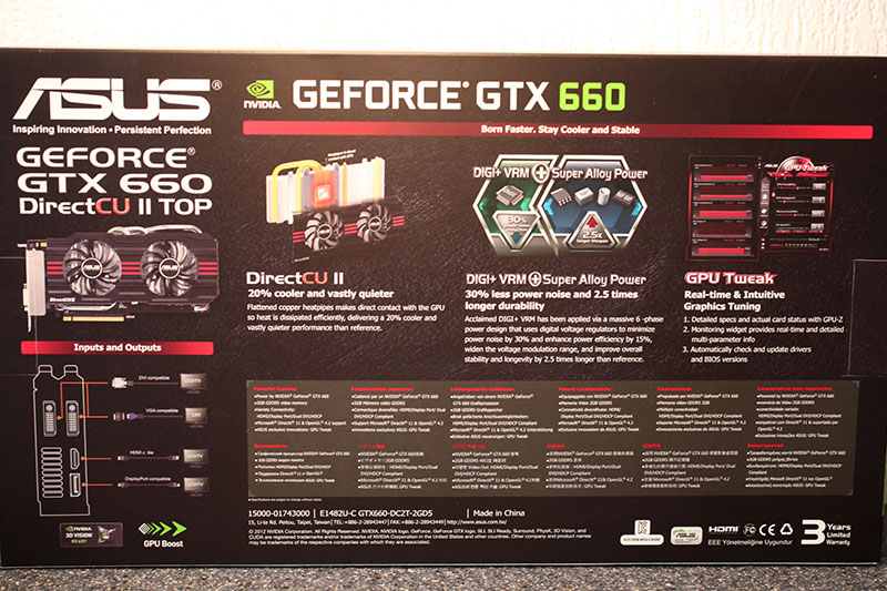
Although NVIDIA has a reference design board for the GeForce GTX 660 in place, its add-in card partners are free to launch graphics cards of their own designs. This review covers the ASUS GeForce GTX 660 DirectCU II TOP, a factory-overclocked graphics card that uses ASUS' popular DirectCU II dual-slot cooling solution, which ASUS has used extensively on GeForce and Radeon based performance-segment graphics cards. The card ships with a core clock speed of 1072 MHz, and 1137 MHz GPU Boost.
| GeForce GTX 650 | GeForce GTX 560 | Radeon HD 6870 | GeForce GTX 560 Ti | Radeon HD 6950 | GeForce GTX 570 | Radeon HD 6970 | Radeon HD 7850 | GeForce GTX 660 | ASUS GTX 660 DCII-T | Radeon HD 7870 | GeForce GTX 580 | GeForce GTX 660 Ti | Radeon HD 7950 | |
|---|---|---|---|---|---|---|---|---|---|---|---|---|---|---|
| Shader Units | 384 | 336 | 1120 | 384 | 1408 | 480 | 1536 | 1024 | 960 | 960 | 1280 | 512 | 1344 | 1792 |
| ROPs | 16 | 32 | 32 | 32 | 32 | 40 | 32 | 32 | 24 | 24 | 32 | 48 | 24 | 32 |
| Graphics Processor | GK107 | GF114 | Barts | GF114 | Cayman | GF110 | Cayman | Pitcairn | GK106 | GK106 | Pitcairn | GF110 | GK104 | Tahiti |
| Transistors | 1300M | 1950M | 1700M | 1950M | 2640M | 3000M | 2640M | 2800M | 2540M | 2540M | 2800M | 3000M | 3500M | 4310M |
| Memory Size | 1024 MB | 1024 MB | 1024 MB | 1024 MB | 2048 MB | 1280 MB | 2048 MB | 2048 MB | 2048 MB | 2048 MB | 2048 MB | 1536 MB | 2048 MB | 3072 MB |
| Memory Bus Width | 128 bit | 256 bit | 256 bit | 256 bit | 256 bit | 320 bit | 256 bit | 256 bit | 192 bit | 192 bit | 256 bit | 384 bit | 192 bit | 384 bit |
| Core Clock | 1058 MHz | 810 MHz | 900 MHz | 823 MHz | 800 MHz | 732 MHz | 880 MHz | 860 MHz | 980 MHz+ | 1071 MHz+ | 1000 MHz | 772 MHz | 915 MHz+ | 800 MHz |
| Memory Clock | 1250 MHz | 1002 MHz | 1050 MHz | 1002 MHz | 1250 MHz | 950 MHz | 1375 MHz | 1200 MHz | 1502 MHz | 1527 MHz | 1200 MHz | 1002 MHz | 1502 MHz | 1250 MHz |
| Price | $110 | $165 | $170 | $200 | $200 | $259 | $380 | $200 | $230 | $250 | $250 | $430 | $300 | $300 |
Packaging

Contents

You will receive:
- Graphics card
- Driver CD + documentation
- DVI adapter
The Card

The ASUS GTX 660 DC II TOP uses a well-working same cooler design we have seen on many ASUS cards recently.

The card requires two slots in your system.
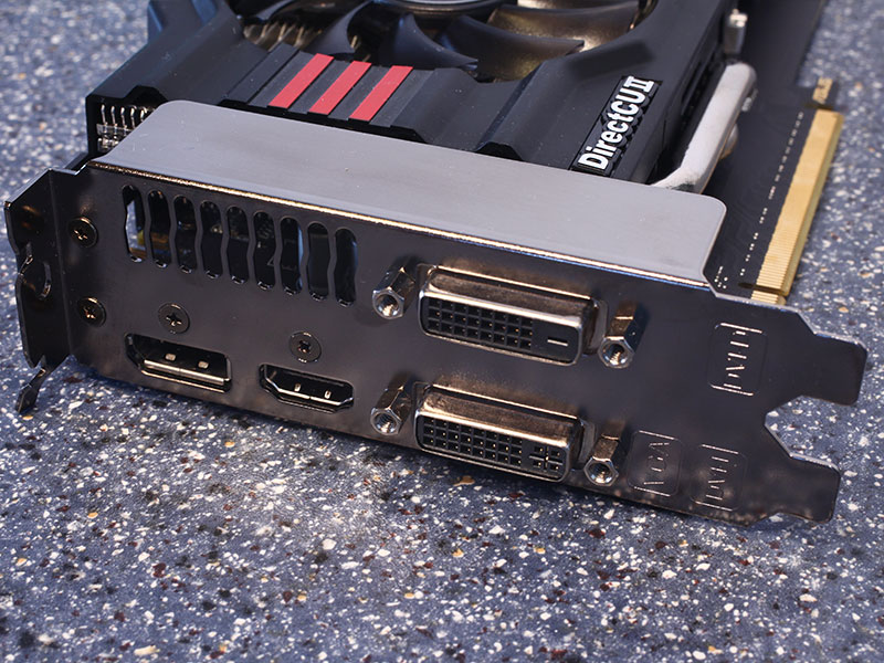
Display connectivity options include two dual-link DVI ports, one full-size HDMI port, and one full-size DisplayPort. You may use all the outputs at the same time.
An HDMI sound device is included in the GPU as well. It is HDMI 1.4a compatible and includes HD audio and Blu-ray 3D movies support. The DisplayPort outputs are version 1.2, which enables the use of hubs and Multi-Stream Transport.
The card has a single SLI connector, which allows a dual-GPU SLI configuration with another GeForce GTX 660.

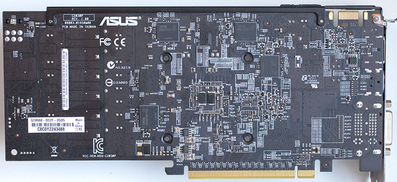
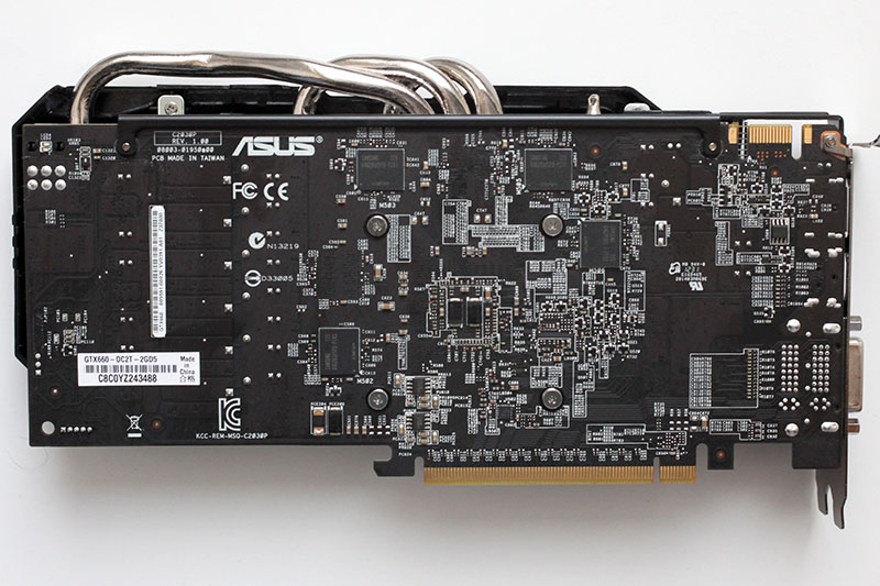
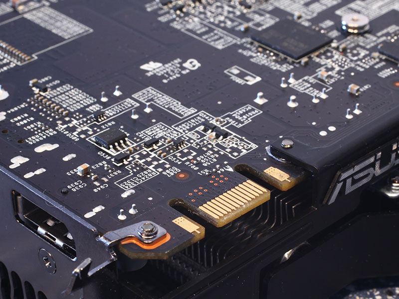
Pictured above are the front and back, showing the disassembled board. High-res versions are also available (front, back). If you choose to use these images for voltmods, etc., please include a link back to this site or let us post your article.
Our Patreon Silver Supporters can read articles in single-page format.
Jul 7th, 2025 15:24 CDT
change timezone
Latest GPU Drivers
New Forum Posts
- Do you still use Antivirus software on your latest hardware? (37)
- Ryzen 9 7950x idles at 55/60C (12)
- 9800x3d temps (40)
- My first build for graphic design, photo & video editing (4)
- R-T-B's PNY RTX 5080 OC Photo sideshow. (16)
- Recommend me a decent budget card :) (22)
- What's your latest tech purchase? (24206)
- PCMA2305 Phase Change Metal Alloy (PCMA) (20)
- About ThrottleStop (3)
- (Need Help!) ERROR: Mismatch at offset Ox00000004 - Expected value: Ox03 - Read back: Ox02 (3)
Popular Reviews
- NVIDIA GeForce RTX 5050 8 GB Review
- Fractal Design Scape Review - Debut Done Right
- NZXT N9 X870E Review
- Sapphire Radeon RX 9060 XT Pulse OC 16 GB Review - An Excellent Choice
- AMD Ryzen 7 9800X3D Review - The Best Gaming Processor
- Upcoming Hardware Launches 2025 (Updated May 2025)
- ASUS ROG Crosshair X870E Extreme Review
- Crucial T710 2 TB Review - Record-Breaking Gen 5
- Sapphire Radeon RX 9070 XT Nitro+ Review - Beating NVIDIA
- PowerColor ALPHYN AM10 Review
TPU on YouTube
Controversial News Posts
- Intel's Core Ultra 7 265K and 265KF CPUs Dip Below $250 (288)
- Some Intel Nova Lake CPUs Rumored to Challenge AMD's 3D V-Cache in Desktop Gaming (140)
- NVIDIA GeForce RTX 5080 SUPER Could Feature 24 GB Memory, Increased Power Limits (115)
- AMD Radeon RX 9070 XT Gains 9% Performance at 1440p with Latest Driver, Beats RTX 5070 Ti (109)
- NVIDIA Launches GeForce RTX 5050 for Desktops and Laptops, Starts at $249 (106)
- Microsoft Partners with AMD for Next-gen Xbox Hardware (105)
- Intel "Nova Lake‑S" Series: Seven SKUs, Up to 52 Cores and 150 W TDP (100)
- NVIDIA DLSS Transformer Cuts VRAM Usage by 20% (97)