 23
23
Samsung 980 Pro 1 TB SSD Review - MLC No More
Test Setup »Packaging
The Drive
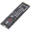
The drive uses the M.2 2280 form factor, which makes it 22 mm wide and 80 mm long.
While most other M.2 NVMe SSDs transfer data over the PCI-Express 3.0 x4 interface, the Samsung 980 Pro connects to the host system over a PCI-Express 4.0 x4 interface, which doubles the theoretical bandwidth.
On the PCB, you'll find the controller, two flash chips, and one DRAM chip; the other side of the PCB is empty.
Samsung has put a little copper foil on the back of the SSD it calls "a heat spreader label to deliver effective thermal control of the NAND chip." Yeah, not really, I doubt it makes any significant difference. It certainly doesn't have much thermal capacity simply because it has so little mass. Also, the hottest component of the drive is the controller chip, not the flash, so the label isn't positioned correctly.
Chip Component Analysis
This is Samsung's new PCIe Gen 4 controller called "Elpis." It is produced on a 8 nm production process in Samsung's foundries, same as NVIDIA's Ampere GPUs. Compared to previous controllers, Elpis can process 128 queues at the same time (Phoenix had 32, UBX only 8).
The two flash chips are Samsung TLC V-NAND v6, which has between 110 and 136 layers. Each chip has a capacity of 512 GB.
A Samsung LPDDR4 chip provides 1 GB of fast DRAM storage for the controller to store the mapping tables.
Jul 2nd, 2025 07:32 CDT
change timezone
Latest GPU Drivers
New Forum Posts
- PCIe 16x does not work (5)
- HTPC Power Consumption Discussion, Upgrade vs Migration (24)
- Need advices with undervolting my I9 13900h, Acer Nitro V15 ANV15-51-93PU (0)
- RTX 5070 discussion (2)
- RX 9000 series GPU Owners Club (1108)
- Help me choose the right PSU , Cooler Master vs Seasonic (63)
- My PSU died.. (3)
- Rare GPUs / Unreleased GPUs (2114)
- RX 580 Cant boot in UEFI, cant disable CSM and cant enable Secure Boot (2)
- With the 4 temperature detection sockets of the Corsair Commander PRO hub, can I skip the ICUE software and directly monitor it with AIDA64? (9)
Popular Reviews
- ASUS ROG Crosshair X870E Extreme Review
- Crucial T710 2 TB Review - Record-Breaking Gen 5
- Sapphire Radeon RX 9060 XT Pulse OC 16 GB Review - An Excellent Choice
- AVerMedia CamStream 4K Review
- Upcoming Hardware Launches 2025 (Updated May 2025)
- AMD Ryzen 7 9800X3D Review - The Best Gaming Processor
- Sapphire Radeon RX 9070 XT Nitro+ Review - Beating NVIDIA
- Lexar NQ780 4 TB Review
- AMD Ryzen 9 9950X3D Review - Great for Gaming and Productivity
- NVIDIA GeForce RTX 5060 8 GB Review
TPU on YouTube
Controversial News Posts
- Intel's Core Ultra 7 265K and 265KF CPUs Dip Below $250 (288)
- NVIDIA Grabs Market Share, AMD Loses Ground, and Intel Disappears in Latest dGPU Update (209)
- Some Intel Nova Lake CPUs Rumored to Challenge AMD's 3D V-Cache in Desktop Gaming (140)
- NVIDIA GeForce RTX 5080 SUPER Could Feature 24 GB Memory, Increased Power Limits (112)
- Microsoft Partners with AMD for Next-gen Xbox Hardware (105)
- NVIDIA Launches GeForce RTX 5050 for Desktops and Laptops, Starts at $249 (105)
- Intel "Nova Lake‑S" Series: Seven SKUs, Up to 52 Cores and 150 W TDP (100)
- NVIDIA DLSS Transformer Cuts VRAM Usage by 20% (92)


