Wednesday, September 30th 2009

NVIDIA GT300 ''Fermi'' Detailed
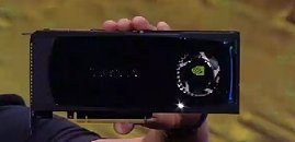
NVIDIA's upcoming flagship graphics processor is going by a lot of codenames. While some call it the GF100, others GT300 (based on the present nomenclature), what is certain that the NVIDIA has given the architecture an internal name of "Fermi", after the Italian physicist Enrico Fermi, the inventor of the nuclear reactor. It doesn't come as a surprise, that the codename of the board itself is going to be called "reactor", according to some sources.
Based on information gathered so far about GT300/Fermi, here's what's packed into it:
Source:
Bright Side of News
Based on information gathered so far about GT300/Fermi, here's what's packed into it:
- Transistor count of over 3 billion
- Built on the 40 nm TSMC process
- 512 shader processors (which NVIDIA may refer to as "CUDA cores")
- 32 cores per core cluster
- 384-bit GDDR5 memory interface
- 1 MB L1 cache memory, 768 KB L2 unified cache memory
- Up to 6 GB of total memory, 1.5 GB can be expected for the consumer graphics variant
- Half Speed IEEE 754 Double Precision floating point
- Native support for execution of C (CUDA), C++, Fortran, support for DirectCompute 11, DirectX 11, OpenGL 3.1, and OpenCL

205 Comments on NVIDIA GT300 ''Fermi'' Detailed
www.nvidia.com/object/gpu_technology_conference.html#livewebcast
A lightly OC'ed gtx 280 beats it even if the 4850 has a 1ghz core OC.
its actually a bit different than you would think.
i like it myself.
these cards will have some serious balls to them from what i've heard in the video so far.
the card is similar to gtx2XX card but slightly smaller
CUDA cores = new term for shader cores for anyone who didn't catch that right away.
Also, that HP netbook doing the HD streaming was pretty sweet (for people watching the webcast).
great name.
that ferrari is pretty nice
And I love the look and the fact that it's shorter than GTX2xx cards. Especially the later.They had started to call them only cores in the last months. Anyway CUDA is (has always be) the name of the architecture itself. Like x86.
What I want to know is if they have shown or will show performance numbers. I now they are not going to be real (like HD5870 being 90% faster than GTX295 lol), but if they say 200% faster you they have something. :laugh:
Btw 280 = 1gb. :rolleyes:
Also there is a patch out there that will allow you to run a higher resolution without having mass amounts of vmem. Whether it lags or not.
www.fudzilla.com/content/view/15758/1/
PD: I've been seing the last part and the augmented reality in the Tegra has really really impressed me.
It defi appears that nVidia might have an ace up their sleeve against the HD5000 series . . . but, all things considered, ATI have yet to throw out any potential date for the release of the 70x2 - leading me to believe they're holding it in the reins until the 300 is out, then slap nVidia with their dual-GPU setup, further driving nVidia's price down . . .
I'm getting the feeling we're going to see a repeat of the HD4000/GT200 release shenanigans - either way, I guess we'll have to see how it goes.
I'd prefer Ati, but i have my own reasons for that. Also a shame that even a i7 cant last up a HD5870 in Crossfire :confused: I think the ball is at eitherway Intel or AMD to produce a much stronger crunching CPU.
Also, there's been no confirmation, nor even rumor, from nVidia regarding a dual-GPU setup . . . actually, most rumors have been a little cautious in that they don't really expect nVidia to have a dual-GPU offering for this series . . . again, though, it's all speculation - nVidia have really yet to offer up much detail straight from their mouth.
Besides, it'd be extremelly shtoopid of nVidia to release a dual-GPU card before releasing anything to stack up against the 5870, especially knowing that ATI still have their dual-GPU monstrosities waiting in the wings . . . it's the same tactic that ATI is currently using, by not releasing the x2 ATM.