Wednesday, January 20th 2010

Galaxy Designs Dual-Core GeForce GTS 250 Graphics Accelerator
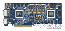
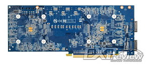
Whereas NVIDIA is inching towards releasing its DirectX compliant GF100 GPU from which it has high expectations, some of its partners don't seem to give up on the two-generation old G92. Galaxy has almost finished designing a graphics card that uses two GeForce GTS 250 GPUs on one PCB, in an SLI on card setup. It refers to the card as "DualCore GTS250", and consists of a long blue PCB which holds two G92-426 GPUs (G92-426 GPUs are used on low-power variants of the GTS 250).
Each GPU is wired to 1 GB of GDDR3 memory across its 256-bit wide memory interface (total 2 GB on board). The two GPUs are connected to the system over an nForce 200 BR-03 bridge chip. The multi-GPU system is contained within the board, with no SLI fingers for expansion, even though G92 chips are Quad SLI capable.The card draws power from two 6-pin PCI-E power connectors, regulated by a 9-phase digital PWM circuit. This isn't the first implementation of its kind from a very technical standpoint. The 2-year old NVIDIA GeForce 9800 GX2 uses two 65 nm G92 chips in a similar implementation, which is Quad SLI capable. There is no word on when Galaxy will release this.
Source:
Expreview
Each GPU is wired to 1 GB of GDDR3 memory across its 256-bit wide memory interface (total 2 GB on board). The two GPUs are connected to the system over an nForce 200 BR-03 bridge chip. The multi-GPU system is contained within the board, with no SLI fingers for expansion, even though G92 chips are Quad SLI capable.The card draws power from two 6-pin PCI-E power connectors, regulated by a 9-phase digital PWM circuit. This isn't the first implementation of its kind from a very technical standpoint. The 2-year old NVIDIA GeForce 9800 GX2 uses two 65 nm G92 chips in a similar implementation, which is Quad SLI capable. There is no word on when Galaxy will release this.


60 Comments on Galaxy Designs Dual-Core GeForce GTS 250 Graphics Accelerator
Look at this G92 first www.overclock3d.net/reviews/gpu_displays/zotac_gts250_amp_1gb_pcie_graphics_card/2
Man, what kind of piece of crap is that? That has got to be one of the worst constructed cards i've ever seen. Everything about that card is cheap and worthless. That cooler, that PCB and I don't even wanna think about the GPU that they used... it probably takes 20, 30$ at most to design that... but that's alright, as long as they still have enough aluminium-plastic and G92s...
Now here's the sad part. Look www.hardwareheaven.com/reviews.php?reviewid=831&pageid=2
Oh no, a CHEAP GTX 285! Oh God take a look at the back of that PCB and that cooler... man that's such a shame to a mighty GPU.
Now go back to the first page here and compare those with this card...
It's the same cheap blue PCB! Let's see Bussmann Choke, a load of power circuits... with no Digital PWM or an overclockable GPU at all LOL. It's won't surprise me if they used all those lowly binned low-power cores and cheap PCB... then believe me that card won't overclock, not even a bit. Maybe 10 or 20 MHZ on the core at most LOL. It won't have any VRM cooling either!
My 9800GX2 at 750+ core will beat it, in both card quality and performance.
This could be a waste of 300$+ and one of the worst cards in history...
HIS and Sapphire uses blue PCB and they make pretty badass cards. Just because its blue dosent mean anything. Its the 2 companies you mentioned here are budget oriented companies.
I see this card as a sad necessity rather than something Galaxy is "happy" to introduce.
It seems the G92b is still widely available and probably quite cheap. Yields should be close to 100% now so even if it's not a 40nm chip, its production price must be cheap.
Its performance should be interesting, nonetheless. They seem to have glued two MXM G92b PCBs together. If this is a <=150€ card, it should successfuly replace the GTX260 in that price point.
Considering how dramatically the heat output that the G92 has decreased I doubt tat this 9800GX2 redux will be expensive.