Monday, March 12th 2012

GK104 Silicon Roughly As Big As G92b
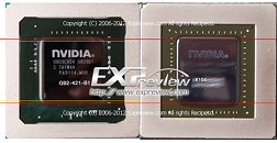
When the first PCB shot of the GK104 reference board surfaced, it sent the punters estimating the die area of the GK104 GPU, which the pinned at somewhere around 320 mm². A newer close-up picture of the GK104, helped calculate the figure more accurately, down to around 300 mm² (±5 mm²). This calculation also takes into account that the GK104 chip-package is as big as that of the G92, and the die just as big. It was compared alongside a 55 nm G92b chip. GK104 is NVIDIA's newest performance GPU built on the Kepler architecture, on which SKUs such as the GeForce GTX 680, are based.
Source:
Expreview

34 Comments on GK104 Silicon Roughly As Big As G92b
1) How dare you suggest W1z can't have a review done in that time frame. W1zz exists in abstract time, he's like the lawnmower man. W1zz could swallow stars and make Galactus look skinny.
2) I'm really really impatient.
3) I have money set aside and a few extra water cooling bits and bobs lying homeless until I finish my loop with a shiny new VGA.
4) I've been holding off buying a 7970 for 2 months, waiting to see what Kepler brings. I just needs to knows!!!!
5) I'm really really impatient.
;)
I really think they've taken that Fermi design, and now hand-tooled it, so I am very eager to see how it all works. A fast enough chip, to me, doesn't need as much cache, as long as it's efficient, and give nthe time between the Fermi launch and now should have been more than enough for them to pull out a killer chip for this gen....so much so that I think I'm going nV this time.
I wasn't very interested in the 7970, to be honest. But these chips...and all this power-control stuff, has me very very interested.I'm just as impatient..I'm just broke. :laugh:
:rockout:
EDIT: In other words, I always went by transistor efficiency. It should be the same or better than Fermi because of various reasons, and never much worse (because you don't change what is not broken, Fermi was on par with Cayman, better than Tahiti). So when it was at least 340mm^2 that meant 3.6-4.0 billion transistors, which against GF110's 3 billions suggested at least 25-40% more performance. With <300mm^2 it's down to ~3 billion, so expecting it to be much much faster than GF110 starts being more unrealistic, or quite a feat if they manage to do it.
Nevertheless, somehow i knew they weren't, going to release a "midrange" part, which could blow 7970 out of the water, regardless of size.
www.overclock.net/t/1225986/tpu-geforce-gtx-680-features-speed-boost-arrives-this-month-etc-etc/400#post_16691060
In short 550$ MSRP and 190W.
:roll:
p.s. The guy is Bs'ing