Wednesday, November 20th 2013

SK Hynix Started Full-Scale Mass Production of 16 nm NAND Flash
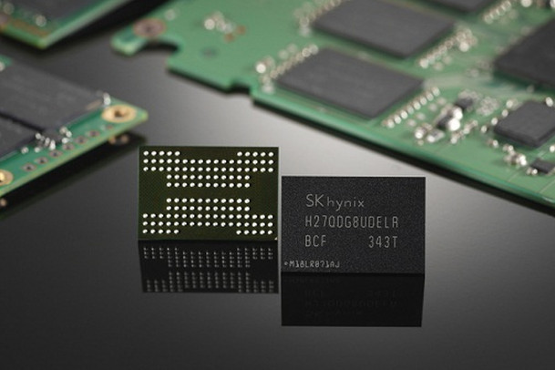
SK Hynix Inc. announced that it has started full-scale mass production of 16 nm 64 Gb (Gigabit) MLC (Multi Level Cell) NAND Flash, which uses the industry's thinnest process technology.
SK Hynix has been mass producing its 1st version of the world's first 16 nm NAND Flash since June and recently has started to mass produce the 2nd version which is more cost competitive due to its smaller chip size. In consequence, the Company geared up for strengthening its competitiveness in NAND Flash. Also, the Company has developed 128 Gb (16 GB, 16 Gigabytes), the highest density in a single MLC chip, based on the specification and endurance of 16 nm 64 Gb MLC. The product is planned to be mass produced from the beginning of next year.
Generally, the thinner process technology shrinks the more frequent interferences among cells occur, but SK Hynix applied up-to-date Air-Gap technology to overcome the interferences among the cells. The Air-Gap technology builds insulation shield with vacuum holes (Air) between circuits not with insulating substances.
"After the Company developed and started to mass produce the industry's thinnest 16 nm product then now prepared high density NAND Flash product portfolio thanks to the development of 16 nm 128 Gb MLC", said senior vice president Jin Woong Kim, the Head of Flash Tech Development. "The Company plans to actively respond to our customers' demands with the NAND Flash products which have high reliability and endurance" he added.
SK Hynix will strengthen its competitiveness in NAND Flash solution while accelerating the development of TLC (Triple Level Cell) and 3D NAND Flash.
SK Hynix has been mass producing its 1st version of the world's first 16 nm NAND Flash since June and recently has started to mass produce the 2nd version which is more cost competitive due to its smaller chip size. In consequence, the Company geared up for strengthening its competitiveness in NAND Flash.
Generally, the thinner process technology shrinks the more frequent interferences among cells occur, but SK Hynix applied up-to-date Air-Gap technology to overcome the interferences among the cells. The Air-Gap technology builds insulation shield with vacuum holes (Air) between circuits not with insulating substances.
"After the Company developed and started to mass produce the industry's thinnest 16 nm product then now prepared high density NAND Flash product portfolio thanks to the development of 16 nm 128 Gb MLC", said senior vice president Jin Woong Kim, the Head of Flash Tech Development. "The Company plans to actively respond to our customers' demands with the NAND Flash products which have high reliability and endurance" he added.
SK Hynix will strengthen its competitiveness in NAND Flash solution while accelerating the development of TLC (Triple Level Cell) and 3D NAND Flash.
1 Comment on SK Hynix Started Full-Scale Mass Production of 16 nm NAND Flash