Monday, March 16th 2015

NVIDIA GeForce GTX TITAN-X Specs Revealed
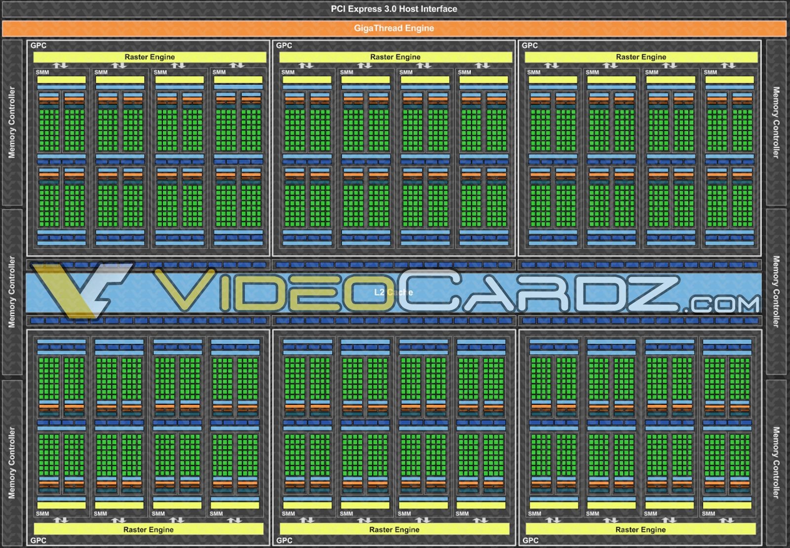
NVIDIA's GeForce GTX TITAN-X, unveiled last week at GDC 2015, is shaping up to be a beast, on paper. According to an architecture block-diagram of the GM200 silicon leaked to the web, the GTX TITAN-X appears to be maxing out all available components on the 28 nm GM200 silicon, on which it is based. While maintaining the same essential component hierarchy as the GM204, the GM200 (and the GTX TITAN-X) features six graphics processing clusters, holding a total of 3,072 CUDA cores, based on the "Maxwell" architecture.
With "Maxwell" GPUs, TMU count is derived as CUDA core count / 16, giving us a count of 192 TMUs. Other specs include 96 ROPs, and a 384-bit wide GDDR5 memory interface, holding 12 GB of memory, using 24x 4 Gb memory chips. The core is reportedly clocked at 1002 MHz, with a GPU Boost frequency of 1089 MHz. The memory is clocked at 7012 MHz (GDDR5-effective), yielding a memory bandwidth of 336 GB/s. NVIDIA will use a lossless texture-compression technology to improve bandwidth utilization. The chip's TDP is rated at 250W. The card draws power from a combination of 6-pin and 8-pin PCIe power connectors, display outputs include three DisplayPort 1.2, one HDMI 2.0, and one dual-link DVI.
Source:
VideoCardz
With "Maxwell" GPUs, TMU count is derived as CUDA core count / 16, giving us a count of 192 TMUs. Other specs include 96 ROPs, and a 384-bit wide GDDR5 memory interface, holding 12 GB of memory, using 24x 4 Gb memory chips. The core is reportedly clocked at 1002 MHz, with a GPU Boost frequency of 1089 MHz. The memory is clocked at 7012 MHz (GDDR5-effective), yielding a memory bandwidth of 336 GB/s. NVIDIA will use a lossless texture-compression technology to improve bandwidth utilization. The chip's TDP is rated at 250W. The card draws power from a combination of 6-pin and 8-pin PCIe power connectors, display outputs include three DisplayPort 1.2, one HDMI 2.0, and one dual-link DVI.
55 Comments on NVIDIA GeForce GTX TITAN-X Specs Revealed
Though if there's not a 4GB 390x, I'll probably sit out this round if the 8GB cards end up at close to 700 USD (which seems to be the suggestion).What's even being tested here? The score number. I understand the basic specifications are being taken from this, but what's being benchmarked?
Each DRAM chip has dedicated dual 128-bit I/O, so four layers = 128 * 2 * 4 = 1024bit. Four HBM stacks surround the GPU on the interposer. The microbumps of solder then connect the HBM stack to interposer and its integrated traces. It will be interesting to see how this effects the pricing with the added complexity, and whether Hynix is doing the final packaging or another third-party manufacturer ( the solder bump pitch should make it an exacting task). I'd assume the HBM+GPU on interposer will then be shipped to AIB's as a complete package.
What surprises me about the whole 390X deal is that benchmarks and specifications arrive at the exact same time as the Titan X / M6000 launch. What are the odds of that happening! :rolleyes:
blogs.nvidia.com/blog/2015/03/16/live-gtc/