Tuesday, May 23rd 2017

Could This be the NVIDIA TITAN Volta?
NVIDIA, which unveiled its faster "Volta" GPU architecture at its 2017 Graphics Technology Conference (GTC), beginning with the HPC product Tesla V100, is closer to launching the consumer graphics variant, the TITAN Volta. A curious-looking graphics card image with "TITAN" markings surfaced on Reddit. One could discount the pic for being that of a well-made cooler mod, until you take a peak at the PCB. It appears to lack SLI fingers where you'd expect them to be, and instead has NVLink fingers in positions found on the PCIe add-in card variant of the Tesla P100 HPC accelerator.
You might think "alright, it's not a fancy TITAN X Pascal cooler mod, but it could be a P100 with a cooler mod," until you notice the power connectors - it has two power inputs on top of the card (where they're typically found on NVIDIA's consumer graphics cards), and not the rear portion of the card (where the P100 has it, and where they're typically found on Tesla and Quadro series products). Whoever pulled this off has done an excellent job either way - of scoring a potential TITAN Volta sample, or modding whatever card to look very plausible of being a TITAN Volta.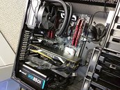
Sources:
Reddit, VideoCardz
You might think "alright, it's not a fancy TITAN X Pascal cooler mod, but it could be a P100 with a cooler mod," until you notice the power connectors - it has two power inputs on top of the card (where they're typically found on NVIDIA's consumer graphics cards), and not the rear portion of the card (where the P100 has it, and where they're typically found on Tesla and Quadro series products). Whoever pulled this off has done an excellent job either way - of scoring a potential TITAN Volta sample, or modding whatever card to look very plausible of being a TITAN Volta.
57 Comments on Could This be the NVIDIA TITAN Volta?
I may be concerned for nothing but I expect the Volta GPUs are going to be more expensive than the Pascals no matter what.
All we've seen so far is a block diagram of Volta.
Meanwhile we are still waiting for Vega, and AMD just talked about taping out Navi at the end of this year. It looks like Vega and Volta will be competing then.
Interesting part for the rumor mill is so hynix announced that they were ramping up hbm2 production for a release of a new graphics card lineup start of 2018.
Now you can take that one of two ways, nvidia will release some nice cards start of 2018 or AMD is further behind than we think.AMD has to release something for it to compete.
Just to add: That's the joke of the 2017 for me. Nothing is going to beat what I read in this thread ever. :)
Stop being delusional. Where did people get this 25-35% faster? deducted from the picture they seen which may not even be Titan Volta or I don't know listening to the aether?
I hope that AMD's Vega shows up and smoke the 1080Ti and blows fanboys pants off. Just for the sake of it :)
That's just silly.
@Caring1 that is linus,he's got a nice following he's good just annoying lol.
www.techpowerup.com/reviews/NVIDIA/GeForce_GTX_1080/30.html
www.techpowerup.com/reviews/NVIDIA/GeForce_GTX_980_Ti/34.html
As far as speculating on Volta Titan I would look at past performance gains for an idea.
Maxwell Titan X was 64% faster than Kepler Titan.
Pascal Titan X was 72% faster than Maxwell Titan X.
It seems reasonable to me to expect similar performance gains with Volta Titan and possibly even more due to the lower process node and new architecture.
@64K and @springs113 , Volta is supposed to be a new architecture, should have more gains that was was previously seen since Kepler (Maxwell was refined Kepler arch).
Remember, all we've seen of Volta so far is just a block diagram.
Volta (15 TFLOP), like Vega (13 TFLOP), is marketed as a deep learning chip. Both companies are bringing versions of it to consumers in (relatively) low volumes.
GV100 will not be a high volume chip, it's huge and the yields wouldn't be that great. GV100 is really pushing the physical limits of the node, and it was originally planned to be made on a smaller node. Not that it's that big of a problem for consumer products though, a GV102 at ~600 mm² would be fine. I still hope that GV102 and GV104 finally will bring full fp16 support though, if used, it can provide a huge boost for gaming.
For that manufacturing process, yeah it won't be high volume chip. First thing what nvidia must deliver is Summit super computer. Summit seems to have six Tesla V100s per node. And it would have ~4600 nodes. That would make 27 600 Tesla V100 for summit super computer(Peak fp64 Petaflops from teslas only is then 207 PFlops). GV100 is huge die so they will need lot of wafers to collect that amount of working dies(TSMC has 12nm FFs in it's 12" gigafabric so it would make appr. 64 dies per wafer at max. If yield are really good that would make ~50 working die per wafer which would need 552 wafers for whole Summit. If Yields are bad like 15 working dies per wafer it would make 1840 wafers to get enough working dies).
Some lucky pioneers got some to play with too:
So yeah, V100 does exist and is out in the wild already.
blogs.nvidia.com/blog/2017/07/22/tesla-v100-cvpr-nvail/