Wednesday, January 17th 2018

Samsung Starts Producing Industry's First 16-Gigabit GDDR6 Memory
Samsung Electronics Co., Ltd., the world leader in advanced memory technology, today announced that it has started mass production of the industry's first 16-gigabit (Gb) Graphics Double Data Rate 6 (GDDR6) memory for use in advanced graphics processing for gaming devices and graphics cards as well as automotive, network and artificial intelligence systems.
"Beginning with this early production of the industry's first 16 Gb GDDR6, we will offer a comprehensive graphics DRAM line-up, with the highest performance and densities, in a very timely manner," said Jinman Han, senior vice president, Memory Product Planning & Application Engineering at Samsung Electronics. "By introducing next-generation GDDR6 products, we will strengthen our presence in the gaming and graphics card markets and accommodate the growing need for advanced graphics memory in automotive and network systems."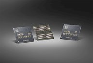 Built on Samsung's advanced 10-nanomter (nm) class process technology, the new GDDR6 memory comes in a 16 Gb density (2 GB), which doubles that of the company's 20-nanometer 8 Gb GDDR5 memory. The new solution performs at an 18-gigabits-per-second (Gbps) pin speed with data transfers of 72 gigabytes per second (GBps), which represents a more than two-fold increase over 8 Gb GDDR5 with its 8 Gbps pin speed.
Using an innovative, low-power circuit design, the new GDDR6 operates at 1.35V to lower energy consumption approximately 35 percent over the widely used GDDR5 at 1.55V. The 10nm-class 16 Gb GDDR6 also brings about a 30 percent manufacturing productivity gain compared to the 20 nm 8Gb GDDR5.
Samsung's immediate production of GDDR6 will play a critical role in early launches of next-generation graphics cards and systems. With all of its improvements in density, performance and energy efficiency, the 16Gb GDDR6 will be widely used in rapidly growing fields such as 8K Ultra HD video processing, virtual reality (VR), augmented reality (AR) and artificial intelligence.
With extensive graphics memory lineups including the new 18 Gbps 16 Gb GDDR6 and recently introduced 2.4 Gbps 8GB HBM2, Samsung expects to dramatically accelerate growth of the premium memory market over the next several years.
"Beginning with this early production of the industry's first 16 Gb GDDR6, we will offer a comprehensive graphics DRAM line-up, with the highest performance and densities, in a very timely manner," said Jinman Han, senior vice president, Memory Product Planning & Application Engineering at Samsung Electronics. "By introducing next-generation GDDR6 products, we will strengthen our presence in the gaming and graphics card markets and accommodate the growing need for advanced graphics memory in automotive and network systems."
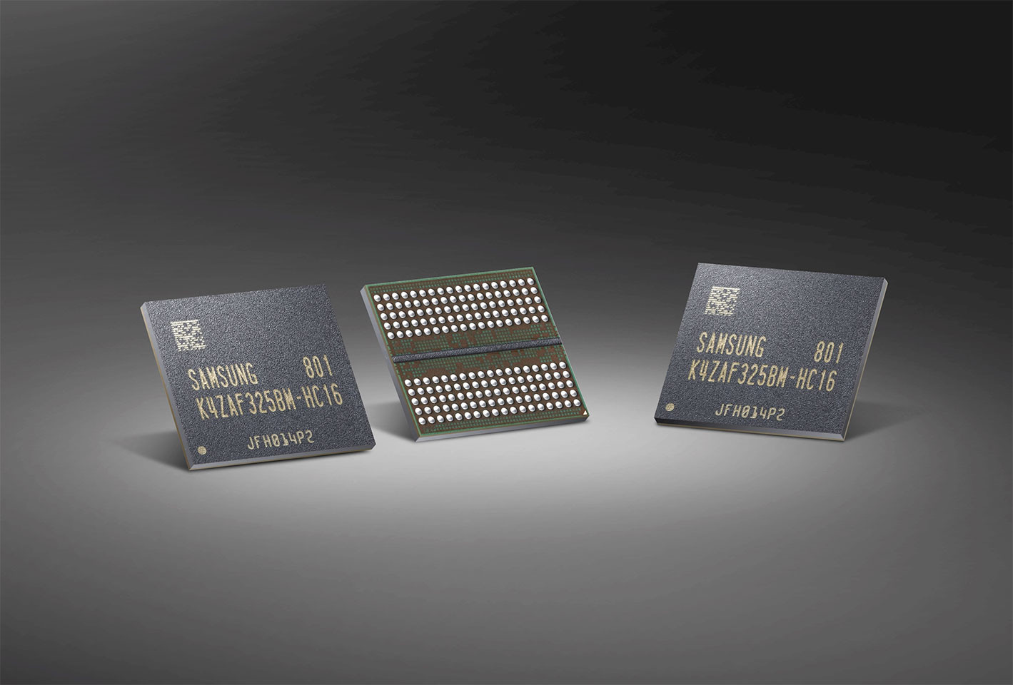
Using an innovative, low-power circuit design, the new GDDR6 operates at 1.35V to lower energy consumption approximately 35 percent over the widely used GDDR5 at 1.55V. The 10nm-class 16 Gb GDDR6 also brings about a 30 percent manufacturing productivity gain compared to the 20 nm 8Gb GDDR5.
Samsung's immediate production of GDDR6 will play a critical role in early launches of next-generation graphics cards and systems. With all of its improvements in density, performance and energy efficiency, the 16Gb GDDR6 will be widely used in rapidly growing fields such as 8K Ultra HD video processing, virtual reality (VR), augmented reality (AR) and artificial intelligence.
With extensive graphics memory lineups including the new 18 Gbps 16 Gb GDDR6 and recently introduced 2.4 Gbps 8GB HBM2, Samsung expects to dramatically accelerate growth of the premium memory market over the next several years.
18 Comments on Samsung Starts Producing Industry's First 16-Gigabit GDDR6 Memory
256-bit GDDR6 with that...
2 Gigabytes * 8 => 16 Gigabytes
72 gigabytes per second * 8 => 576 gigabytes per second.
vs
HBM2 Plus
(1024 * 2.4) divided by 8 => 307.2 gigabytes per second with 8 gigabytes and 614.4 gigabytes per second for 16 gigabytes.
19.2/38.4 gigabytes per second isn't a huge loss, HBM2 is good as dead.
Your logic is as good as dead, don't worry HBM is not going anywhere. What's funny is that Samsung themselves are developing HBM3 which is supposed to reach 512GB/s per stack.
Low manufacturing cost + high availability + Satisfying performance = winning products
HBM type has far, far greater issues. At least on nvidia's side, GDDR5X based products get high scores.
This is the first time we see 2GB of VRAM per chip. Something as small as the area of a SODIMM is enough to give 8GBs of VRAM into a chip.
Definitely on the compact side
I think the reason why nvidia is creating ampere is to maximize profits in the long run. They'd rather spend money on R&D for a 300mm2 GTX2080 than produce a 400mm2 volta for gamers. I think they're initially going to to aim for 1080Ti performance at $550 with a 300mm2 chip rather than a 20% faster card at $650, like 980Ti->1080. Why ? I think they'd like to sell amprere in 2018 and ampere refresh in 2019, let AMD be the guinea pig with multi chip design.
That's why I think we might see a 2080 with 12GB DDR6, 72 ROPs, 2880 sp, performance at 1080Ti level. Impossible you say ? I think it's well possible considering that might clock +2GHz out of the box and volta has already shown some improvement over pascal in dx12 async games (like sniper 4). That, combined with efficiency and cost, will be the main selling point for the new cards. 1080Ti's are crazy ovepriced now due to mining, if nvidia launched 2080 with 1080Ti performance in dx12 and 90-95% of 1080Ti in dx11 at $100-150 less than 1080Ti gamers would be more than content.
On the other hand, while memory bus widths have gone down, 384-bit is still used on high-end cards and 512-bit is not unheard of (AMD did that as recently as Hawaii).
384-bit GDDR6 would be 864 GB/s
512-bit GDDR6 would be 1152 GB/s
HBM is definitely a large part to play in the future but there will be alternatives.What do you mean? HBM stacks? V100 has 4 stacks and 128 ROPs. 32 ROPs per stack?
Edit: Oh, you're right. The entire Pascal range has 8 ROPs per each 32-bit of VRAM. That should not be a hard limit in any way but just an architectural (or perhaps optimization) choice.
Why do you think Nvidia put HBM on Volta already?
Why do you think Intel and AMD are using HBM on their new chip?
The memory cells are exactly the same, the silicon is the same if it were GDDR or HBM or whatever, it's traces and resist, nothing magical happens to one and not the other. The only difference is one is packaged and bumped, the other is left as a silicon substrate and bumped.
i never obsessed over bandwidth, obviously every gen is going to raise it, but not every gen or type allows stacking & space saving