Monday, February 19th 2018

Intel Unveils Discrete GPU Prototype Development
Intel is making progress in its development of a new discrete GPU architecture, after its failed attempt with "Larrabee" that ended up as an HPC accelerator; and ancient attempts such as the i740. This comes in the wake of the company's high-profile hiring of Raja Koduri, AMD's former Radeon Technologies Group (RTG) head. The company unveiled slides pointing to the direction in which its GPU development is headed, at the IEEE International Solid-State Circuits Conference (ISSCC) in San Francisco. That direction is essentially scaling up its existing iGPU architecture, and bolstering it with mechanisms to sustain high clock speeds better.
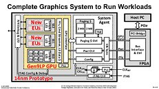
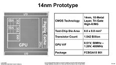
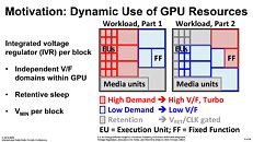
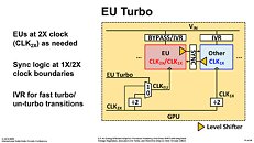
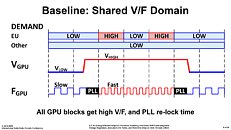
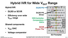
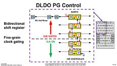
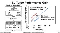
The company's first 14 nm dGPU prototype, shown as a test-chip at the ISSCC, is a 2-chip solution. The first chip contains two key components, the GPU itself, and a system agent; and the second chip is an FPGA that interfaces with the system bus. The GPU component, as it stands now, is based on Intel's Gen 9 architecture, and features a three execution unit (EU) clusters. Don't derive numbers from this yet, as Intel is only trying to demonstrate a proof of concept. The three clusters are wired to a sophisticated power/clock management mechanism that efficiently manages power and clock-speed of each individual EU. There's also a double-clock mechanism that doubles clock speeds (of the boost state) beyond what today's Gen 9 EUs can handle on Intel iGPUs. Once a suitable level of energy efficiency is achieved, Intel will use newer generations of EUs, and scale up EU counts taking advantage of newer fab processes, to develop bigger discrete GPUs.More slides follow.
Source:
PC Watch
The company's first 14 nm dGPU prototype, shown as a test-chip at the ISSCC, is a 2-chip solution. The first chip contains two key components, the GPU itself, and a system agent; and the second chip is an FPGA that interfaces with the system bus. The GPU component, as it stands now, is based on Intel's Gen 9 architecture, and features a three execution unit (EU) clusters. Don't derive numbers from this yet, as Intel is only trying to demonstrate a proof of concept. The three clusters are wired to a sophisticated power/clock management mechanism that efficiently manages power and clock-speed of each individual EU. There's also a double-clock mechanism that doubles clock speeds (of the boost state) beyond what today's Gen 9 EUs can handle on Intel iGPUs. Once a suitable level of energy efficiency is achieved, Intel will use newer generations of EUs, and scale up EU counts taking advantage of newer fab processes, to develop bigger discrete GPUs.More slides follow.







65 Comments on Intel Unveils Discrete GPU Prototype Development
If they leverage the experience they have putting an Fpga to work in the data center they could have a Computer accelerator instead of just a graphics or compute accelerator.
After all the ease of reconfiging FPGAs make them the ultimate possible accelertor of Anything.
This could sidestep any graphics performance gap by increasing common addoption of fpga APIs obviously within direct X.
All chip companies are both diversifying and adopting more modular, many accelerator designs ,an fpga usurps a lot of that in one package so it's only time before we see them in consumer land.
All opinions on possibilities, too early to know tbh.
i740 was a terrible GPU even for the day. It would be like calling a gtx 1030 a good midrange gpu.
Intel can not make a GPU and never will because it's a CPU company first.
My "Yes" vote was reserved and contingent on the idea that Intel is going to be competitive in the entry and mid-tier levels, which currently they aren't.
There were side-by-side comparisons of a GTX 650 and a Iris Pro graphics where they said "You can't tell the difference!" Then they announced they had a GPU with double the EU's coming out the next generation (Clearly trying to infer that they would be in the midrange segment for the first time ever). They wanted to get to the level where they could be in most gaming laptops, but they couldn't and so AMD is providing them with their Vega Gx products.
P.S. Also keep in mind that even to get to "GTX 650 levels," Intel had to include ludicrously expensive EDRAM. So sure they beat AMD for a year by ~30%, but their product was using 14nm instead of 28nm; and it cost 2-3x as much to make lol. That's not sustainable....
I'll agree with other comments in this thread that I'd be hard pressed to believe they will catch up to nVidia anytime soon but if they release something I can almost guarantee it will be something interesting and different.
They could have use just THAT dumb expenditure to make an entire GPU line-up, or possibly even a new CPU architecture that wouldn't have been Curb Stomped by Zen...
1 - It doesn't serve their strategy to diversify into the discrete desktop GPU market
2 - Their development focus is in low-power, mobile devices. Shifting to desktop discrete might upset the status quo and the investment outlook.
3 - Their GPU strategy is to supplement their SoC strategy in exclusivity (i.e. Adreno)
4 - reasons...
Basically you need someone with big balls and deep pockets to take on the power that be...
1) Why a dual chip solution? Why separate the computer interfacing completely from the GPU? Was one chip borrowed from some other project (e.g. wifi controller) so they saved time/money by piggybacking on the basics of existing tech? This doesn't make sense by itself.
2) They are really focused on keeping power consumption to a minimum. This point is particularly interesting because it tells us where their focus is: portable/low power devices. My first thought was Atom+4K which they're already doing. Second thought is that Intel is very concerned about Vega M powered Ryzen chips. That doesn't explain why Intel is pursuing discreet graphics though.
Then it struck me: Intel wants to divorce themselves completely from NVIDIA which means no more Intel/NVIDIA Optimus systems. AMD sucks right now in the laptop GPUs market so, other than crawling back to NVIDIA, Intel's only option is to scale up their IGPs to match NVIDIA's in gaming/workstation laptops.
Circling back to #1, why the two chip solution? Intel owns the CPU and chipset. They're soon going to own the GPU too. Intel likely kept them separate so they could create a new interface (replacing the generic PCIE controller) tailored to the dual GPU configuration (IGP + IGP expansion card). In a corporate environment, IT could order 100 units of the same computer with 20 IGP expansion cards then only add the card to computers that are destined for people that need it. Presumably there is no additional set up and to the operating system, it will only see one GPU with expanded capabilities. The IGP can enable/disable EU clusters as demand increases/decreases.
It makes perfect sense. i7-8809G may have tested that new interface too. They could also package the MCM on a PCB to be hooked into desktop PCIE slots. I'm still thinking there has to be something unique about the PCIE implementation here--perhaps a dedicated low latency slot that removes most of the overhead by having a dedicated and constrained PCIE controller (only talks to one device).
In the old days you'd have CPU+North Bridge+South Bridge, then Intel moved the north bridge onto the CPU. CPUs now have their own memory controller, PCIe controller, etc... That's what Intel is used to doing.
In this case, from what they're showing here, it seems they are using a modular design for expedience to show the proof of concept. Whatever route they take down the line will determine if this will be a single piece of silicon or a bunch of chips soldered together.
However, don't cream your pants just yet. This PoC is not a new architecture but a tweaked Gen9LP chip (HD Graphics 5xx-series) attached to a system agent, and with integrated voltage regulators to better manage power and frequencies... they're just trying to optimize efficiency, rather than create an entirely new GPU design. Apparently they have low-power cores and *cough* "high-performing" *cough* cores (EUs), much like ARM has light- and heavy- workload cores. This design doesn't change anything architecturally (i.e. the GPUs are as crappy as before), but it does bring in power savings and extended battery life (where battery life is relevant).
Superimpose this on the PCIe interface and you can optimize any type of interface: EMIB, add-in card, etc...
It's a bit "meh" to be honest, but Raja probably told people they needed to do *something* for IEEE.
I said in that post , did you read one line.
Play fair dude, this is likely Raja's very first step towards something,
"ie intels present best igpu with hybrid shaders and an fpga added to make up for all thats missing if they don't fit cpu cores and more importantly the rest of its supporting circuitry related to specific purposes ie power control but, the fpga mainly acts as an interface between intels proprietary inter chip interface type and pciex since it's clear the igpu was designed without pciex in mind it makes sense to test what they can expect before scaling up the design, they won't actually make many of these even for themselves, it's a stepping stone chip clear as day."
Also
The shop bought ones four or five years out imho and certainly won't be a dual chip solution maybe MCM though.
Because that FPGA could possibly be a game changer if used to pump the GPUs core performance intelligently and or to directly affect a new Api for mainstream use case acceleration, intel already do fpga in server so they know it's got legs.
Later on i said this too,
im half expecting something a bit more now I've seen this.
If they leverage the experience they have putting an Fpga to work in the data center they could have a Computer accelerator instead of just a graphics or compute accelerator.
After all the ease of reconfiging FPGAs make them the ultimate possible accelertor of Anything.
This could sidestep any graphics performance gap by increasing common addoption of fpga APIs obviously within direct X.
All chip companies are both diversifying and adopting more modular, many accelerator designs ,an fpga usurps a lot of that in one package so it's only time before we see them in consumer land.
So i clearly get that Raja grabbed whatever was near, it didn't have external connections just inter chip ones so they added an fpga ,which coincidentally could be a viable co processor itself.
Seams another news agro site agrees with me but they have the name of purpose.
Edge computing ,not Gaming per say , that would be a shame.