Tuesday, March 27th 2018

NVIDIA Announces World's Most Powerful Professional GPU - The Quadro GV100
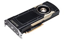
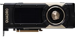
NVIDIA CEO Jensen Huang today announced to the world what is being touted as the world's most advanced GPU for professionals - the Quadro GV100. Based on NVIDIA's Volta architecture and sporting 5,120 CUDA cores, this is a behemoth of a professional graphics card, eclipsing all previous NVIDIA offerings by a wide margin.
The GV100 was built to usher in all kinds of workload performances - from machine learning and HPC to actually being the only professional graphics card actually capable of processing workloads around the just announced RTX raytracing suite. That alone is a boon that's sure to get these cards moving from the presses and unto professional's hands all the faster. The 5,120 CUDA cores join the 32 GB of HBM2 memory and up to 7.4 TFLOPs of power for double-precision rendering, 14.8 TFLOPs for single-precision workloads, 29.6 TFLOPs half-precision, and 118.5 TFLOPs for deep learning through its Tensor Cores. The previous high-end Quadro, the GP100, offered 10.3 TFLOPs for single-precision rendering.This graphics card is a behemoth in all senses. The 5,120 CUDA cores, 640 Tensor cores, 320 texture units and 128 ROPs of hardware on this GPU run at some 1450 MHz boost clocks. The HBM 2 memory is a 1.7 Gbps affair on a 4096-bit bus, which naturally features ECC (error correction for data-critical workloads). The TDP stands at a (relatively) innocuous 250 W - for this big a chip, it's actually rather tame, and could make it (mostly a drop-in replacement for the Quadro P100, which sports TDP a tad lower at 230 W.The Quadro GV100 has dropped the GP100's sole DVI port, leaving it with 4x DisplayPort 1.4 connectors. The card also features standard Quadro Sync and Stereo connectors for synchronized refresh and quad-buffered stereo respectively. Naturally, this Quadro GV100 features support for dual NVIDIA NVLink operation, which will allow prospective users to enjoy the full benefits of the interface, particularly low latency data transfers, remote memory access, and memory pooling.
Sources:
EnGadget, AnandTech
The GV100 was built to usher in all kinds of workload performances - from machine learning and HPC to actually being the only professional graphics card actually capable of processing workloads around the just announced RTX raytracing suite. That alone is a boon that's sure to get these cards moving from the presses and unto professional's hands all the faster. The 5,120 CUDA cores join the 32 GB of HBM2 memory and up to 7.4 TFLOPs of power for double-precision rendering, 14.8 TFLOPs for single-precision workloads, 29.6 TFLOPs half-precision, and 118.5 TFLOPs for deep learning through its Tensor Cores. The previous high-end Quadro, the GP100, offered 10.3 TFLOPs for single-precision rendering.This graphics card is a behemoth in all senses. The 5,120 CUDA cores, 640 Tensor cores, 320 texture units and 128 ROPs of hardware on this GPU run at some 1450 MHz boost clocks. The HBM 2 memory is a 1.7 Gbps affair on a 4096-bit bus, which naturally features ECC (error correction for data-critical workloads). The TDP stands at a (relatively) innocuous 250 W - for this big a chip, it's actually rather tame, and could make it (mostly a drop-in replacement for the Quadro P100, which sports TDP a tad lower at 230 W.The Quadro GV100 has dropped the GP100's sole DVI port, leaving it with 4x DisplayPort 1.4 connectors. The card also features standard Quadro Sync and Stereo connectors for synchronized refresh and quad-buffered stereo respectively. Naturally, this Quadro GV100 features support for dual NVIDIA NVLink operation, which will allow prospective users to enjoy the full benefits of the interface, particularly low latency data transfers, remote memory access, and memory pooling.


20 Comments on NVIDIA Announces World's Most Powerful Professional GPU - The Quadro GV100
Quadro GV100
Boost Clock: 14.817TFLOPs + 118.538TFLOPs = 133.335TFLOPs
TITAN V
Boost Clock: 14.899TFLOPs + 119.193TFLOPs = 134.092TFLOPs
People who train machines know how much
The Register: 2 + 2 = 4, er, 4.1, no, 4.3... Nvidia's Titan V GPUs spit out 'wrong answers' in scientific simulations
Nice card though.
Not really sure why, tbh, the Titan V even exists apart from making some quick bucks from eager early adopters.
TPU: NVIDIA Forbids GeForce Driver Deployment in Data Centers
Be funny if Titan line evolves to be the mining card
There is always a chance, I suppose.
From Nvidia:
“All of our GPUs add correctly. Our Tesla line, which has ECC [error-correcting code memory], is designed for these types of large scale, high performance simulations. Anyone who does experience issues should contact support@nvidia.com.”
Start hiring xD @W1zzard
Everyone is jumping to a hardware fault conclusion when as usual, none of us know. From what I read, it's also a very specific calculation and one could argue, ECC, available on proper (not gimmicky Titan brand) hardware would render this error void.
From the Register itself:
A spokesperson for Nvidia has been in touch to say people should drop the chip designer a note if they have any problems. The biz acknowledged it is aware of at least one scientific application – a molecular dynamics package called Amber – that reportedly is affected by the Titan V weirdness
Storm, teacup and Nvidia will fix.
What I'm interested in, is how this handles RTX. But I guess it will be a while before someone manages to get a hold of both the hardware and the software needed to benchmark that.