Tuesday, May 15th 2018
International Memory Workshop: 3D NAND Flash to Reach 140 Layers By 2021
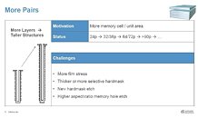
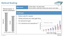
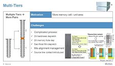
3D NAND has been one of the most important new technologies in allowing for greater storage density in space-constrained hardware (isn't that always the case, though?) As we've stepped away from the usual 2D NAND to the nowadays market-leading 3D solutions, which stack layers of memory one on top of the other (thus making use of vertical space instead of the usually more costly horizontal one), memory density and price per GB has been steadily declining - a relationship that isn't quite as parallel as it may seem, but still occurs.Applied Material's Sean Kang, speaking at Japan's International Memory Workshop (IMW), said that he expects future 3D NAND technologies to achieve 140 layers (up from today's leading 64-layer tech) by 2021. Increased numbers of layers will allow for increased die densities whilst keeping the same PCB real-estate and implementation area; at the same time, which is something the industry is craving for as data-sets only continue to increase in size. Before 2021 and its 140-layer NAND comes (which will require new fabrication materials), 90-layer solutions are expected to be launched this year, with a 20% decrease in layer height, down from its current 60 nm to 55 nm, which will allow for relatively stable stack heights, even as the number of layers increases significantly (by around 40% compared to 64-layer tech). Cheaper, more dense NAND tech - what isn't there to like?
Sources:
via ComputerBase.de, PC Watch


11 Comments on International Memory Workshop: 3D NAND Flash to Reach 140 Layers By 2021
:fear:
Actually curious of what the thermal profile is on a 140-layer NAND chip.
The capacity gains alone will be worth it.