Wednesday, October 10th 2018

TSMC 7 nm Second-Generation EUV Chips Taped Out, 5 nm Risk Production in April 2019
TSMC, the world's biggest contract semiconductor manufacturer, who is at the forefront of 7 nanometer production has just announced that they are making good progress with their second generation of 7 nm technology "N7+", using EUV (Extreme Ultraviolet Lithography). A first design for N7+ from an unnamed customer has been taped out. The company's first-gen 7 nm production is running well already, with final products, like Apple iPhone already in the hands of customers.
While not fully EUV yet, the N7+ process will see limited EUV usage, for up to four non-critical layers, which gives the company an opportunity to figure out how to make best use of the new technology, how to ramp up for mass production and how to fix the little quirks that show up as soon as you move from the lab to the factory.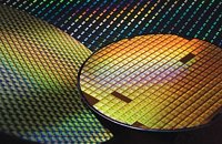 The new technology is expected to bring 6-12% lower power and 20% better density, which could be especially important for power and heat constrained designs. It will also be a good marketing vehicle for many of TSMC's customers who are expected to release new designs every year. With the N7+ process, TSMC is targeting the automotive sector, too, where releases happen more slowly, which suggests that this process will be available for a long time.
Moving beyond 7 nanometers, TSMC's target is 5 nm, internally called "N5". This process will use EUV for up to 14 layers and is expected to be ready for risk production in April 2019. According to TSMC, many of their IP blocks are ready for N5, with the exception of PCIe Gen 4 and USB 3.1. We have all been waiting for PCIe Gen 4 on new GPUs and it looks like we'll have to wait even longer for this new version to become available. Compared to the N7 designs, which have initial costs in the $150 million range, the cost for N5 is expected to increase even further, up to $200 to $250 million.
Source:
EETAsia
While not fully EUV yet, the N7+ process will see limited EUV usage, for up to four non-critical layers, which gives the company an opportunity to figure out how to make best use of the new technology, how to ramp up for mass production and how to fix the little quirks that show up as soon as you move from the lab to the factory.

Moving beyond 7 nanometers, TSMC's target is 5 nm, internally called "N5". This process will use EUV for up to 14 layers and is expected to be ready for risk production in April 2019. According to TSMC, many of their IP blocks are ready for N5, with the exception of PCIe Gen 4 and USB 3.1. We have all been waiting for PCIe Gen 4 on new GPUs and it looks like we'll have to wait even longer for this new version to become available. Compared to the N7 designs, which have initial costs in the $150 million range, the cost for N5 is expected to increase even further, up to $200 to $250 million.
22 Comments on TSMC 7 nm Second-Generation EUV Chips Taped Out, 5 nm Risk Production in April 2019
It's not HVM (High Volume Manufacturing), it's risk production where each IC manufacturer makes a few hundred test wafers to test the final silicon in their labs and to sample its partners that integrate it in their products.
We won't see 5nm HVM until Q2 2020 and actual silicon in products in Q3/Q4 2020 (probably, as it happened for the last 2-3 years, in the 2020 iPhone).
Very misleading this title and information is.
maybe I can fix it for you: "Nvida RTX 5nm in April 2019, Confirmed!" :D
And 5nm mass production in April 2019 is not feasible.
7 nm features 1.6X logic density than 10 ~~100 Mtr/mm2
10 nm 2X logic density than 12/16nm ~~60 Mtr/mm2
We are at 1.2X1.6X2 ~ 4X better logic density at this point in time, and still not getting it in real GPU products.
All we have for now is 12/14/16 nm with ~~30 Mtr/mm2.
yeah this means RTX 2080Ti 754mm2 the size of GTX 1060 with 200mm2 if tape out next year.
Hmm, I see that the original source says 'risk' which is wrong, unless they are trying to say, very poorly I might add, that production of 5 nm is AT RISK, which of course they are not saying.
TSMC and GloFo 16/14/12nm => TSMC 7nm allows up to 3-4× increased density, but it also limited by W/mm², and the clocks they want to run the chip on.
EUV has around 15 times smaller wavelength compared to DUV which allows for smaller features. The actual devices do 30-50% smaller resolution compared to DUV devices.
There are downsides and challenges both technical as well as getting enough EUV devices to run volume production.From what TSMC has disclosed, Intel's 10nm should be in between TSMC's N7 and N7+ in most metrics.
It will be interesting to see when EUV are fully adapted, maybe we will even move into 5nm territory by that time.