Thursday, March 21st 2019

Intel Gen11 Architecture and GT2 "Ice Lake" iGPU Detailed

Intel "Ice Lake" will be the company's first major processor microarchitecture since the "Skylake" (2015), which promises CPU IPC improvements. Intel has been reusing both CPU cores and graphics architecture for four processor generations, since "Skylake". Gen9 got a mid-life update to Gen9.5 with "Kaby Lake", adding new display interfaces and faster drivers. "Ice Lake" takes advantage of the new 10 nm silicon fabrication process to not just pack faster CPU cores (with increased IPC), but also the new Gen11 iGPU. Intel published a whitepaper detailing this architecture.

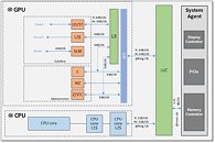
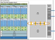
An illustration in the whitepaper points to the GT2 trim of Gen11. GT2 tends to be the most common variant of each Intel graphics architecture. Gen9.5 GT2, for example, is deployed across the board on 8th and 9th generation Core processors (with the exception of the "F" or "KF" SKUs). The illustration confirms that Intel will continue to use their Ring Bus interconnect on the mainstream implementation of "Ice Lake" processors, despite possible increases in CPU core counts. This is slightly surprising, since Intel introduced a Mesh interconnect with its recent HEDT and enterprise processors. Intel has, however, ensured the iGPU has a preferential access to the Ring Bus, with 64 Byte/clock reads and 64 Byte/clock writes, while each CPU core only has 32 Byte/clock reads and 32 Byte/clock writes.
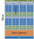
While the CPU core ring-stop terminates at its dedicated L2 cache, for the iGPU, it does so at a component called "GTI", short for graphics technology interface. The GTI interfaces with two components: Slice Common and a L3 cache which is completely separate from the processor's main L3 cache. The iGPU now has a dedicated 3 MB L3 cache, although the processor's main L3 cache outside the iGPU is still town-square for the entire processor. The iGPU's L3 cache cushions transfers between the GTI and Subslices. These are the indivisible number-crunching clusters of the GPU, much like streaming multiprocessors on an NVIDIA GPU - this is where the shaders are located. In addition to the subslices we find separate geometry processing hardware, and front-ends, including fixed-function hardware to accelerate media, which all feed into the eight subslices. The back-end is handled by "Slice Common", which includes ROPs, which write to the iGPU's own L3 cache.

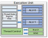
Each Subslice begins with an instruction cache and thread dispatch that divides the number-crunching workload between eight execution units or EUs. Gen11 GT2 has 64 EUs, which is a 166% growth over the 24 EUs that we saw with Gen9.5 GT2 (for example on Core i9-9900K). Such a significant increase in EUs will probably double performance, to make up lost ground against AMD's Ryzen APUs. Each EU packs two ALUs with four execution pipelines each, register files, and a thread control unit. Certain other components are shared between the EUs, such as media samplers. Intel is updating the media engine of its integrated graphics to support hardware acceleration of more video formats, including 10-bpc VP9. The display controller now supports Panel Self Refresh, Display Context Save and Restore, VESA Adaptive-Sync, and support for USB-C based outputs.
Add your own comment

27 Comments on Intel Gen11 Architecture and GT2 "Ice Lake" iGPU Detailed

#1
Bones
I'm waiting to see the performance percentage increase and the pricetag with it.
That's all I can say ATM because I"m not expecting anything much different than what's been before.

If the percentage increase is good that would be great, esp if the pricetag for it doesn't amount to wallet-rape.
Posted on Reply
#3
W1zzard
BonesI'm waiting to see the performance percentage increase
From that EU increase I'd expect around 2x the perf vs current Intel iGPU
Posted on Reply
#4
Bones
That would be excellent to see, a real benefit derived from what competition does for the industry (And end user). Competition from AMD has had a good effect for everyone, pushes development and maybe we'll see some of the benefits of such with this release.

I'm still wondering about what the pricetag would be, hopefully good but that's something we have no real control over except by voting with our wallets come release time.
Posted on Reply
#5
londiste
24 EU Gen9.5 (UHD 630 and the ilk) is 192 shaders.
64 EU Gen11 is 512 shaders.
Architectural changes aside, this is over 2.5 times the compute power.
Posted on Reply
#6
Ferrum Master
londiste24 EU Gen9.5 (UHD 630 and the ilk) is 192 shaders.
64 EU Gen11 is 512 shaders.
Architectural changes aside, this is over 2.5 times the compute power.
They could lower the clock to tame the heat. So actually power envelope is the deciding factor. The perf increase thus can be lower than 2.
Posted on Reply
#7
W1zzard
Ferrum MasterThey could lower the clock to tame the heat. So actually power envelope is the deciding factor. The perf increase thus can be lower than 2.
This, and also workloads don't scale with cores linearly, which is part of GCN's problem.

I think ~2x is a reasonable estimate though
Posted on Reply
#8
Bones
Have to agree - On paper it well could be 2.5x the computing power but will it actually deliver?
And final specs (Clockspeeds) I'd have to think aren't exactly set in stone just yet, esp if during development they run into problems like before and are forced to tweak things so it works without issues in the end.

Much work to be done yet with it.
Posted on Reply
#9
GorbazTheDragon
Unless they are really far behind the curve from the efficiency standpoint, memory bandwidth will probably be more restrictive than anything else. You'd be surprised how many laptops only use a single memory channel.

I wonder if they will revisit eDRAM or maybe have a go atHBM any time soon. Alternatively 3-channel memory could also be an option.
Posted on Reply
#10
dj-electric
Having eDRAM in some graphically boosted parts could be amazing...
Posted on Reply
#11
Countryside
Interesting is the new instruction set AVX 512 it could give a great performance boost to video editing.
Posted on Reply
#12
R0H1T
BonesHave to agree - On paper it well could be 2.5x the computing power but will it actually deliver?
And final specs (Clockspeeds) I'd have to think aren't exactly set in stone just yet, esp if during development they run into problems like before and are forced to tweak things so it works without issues in the end.

Much work to be done yet with it.
Yes but extra compute power doesn't always translate into gaming/graphics as we've seen with AMD. There are other bottlenecks including bandwidth & the underlying uarch, having said that L1 & L2 changes made a huge difference for Nvidia - maybe that'll be enough for Intel to complete?
Posted on Reply
#13
londiste
R0H1Thaving said that L1 & L2 changes made a huge difference for Nvidia - maybe that'll be enough for Intel to complete?
Only L3 cache is bigger, rest are exactly the same. In fact, there do not appear to be that many changes on the GPU side of things. Largely the same EUs, same caches (except the larger L3). The only major change to GPU itself is the added EUs and twice the ROPs?
Posted on Reply
#14
Vayra86
Article speaks of IPC improvements, but I have a hard time identifying those for CPU tasks. Sure, the GPU will be more zippy, but we ain't got time for that low-end junk.

Bottom line I think is a minor clock bump for CPU along with substantial IGP improvements. Broadwell v2... Inb4 another 5775C that will be a rare unicorn in the wild. Given Intel's 10nm woes, that seems plausible...
Posted on Reply
#15
londiste
Vayra86Sure, the GPU will be more zippy, but we ain't got time for that low-end junk.
The GPU configuration they present as Gen11 GT2 is roughly equal to the current Vega8. Intel GT2 is in a lot of laptops.
Posted on Reply
#16
Vayra86
londisteThe GPU configuration they present as Gen11 GT2 is roughly equal to the current Vega8. Intel GT2 is in a lot of laptops.
Oh don't get me wrong, sure there's a market, its just not me, or any enthusiast I reckon. The IGP will never become fast enough to truly rival dedicated cards, those goal posts move every release anyway and there is a fundamental TDP problem with APUs.
Posted on Reply
#17
R0H1T
londisteIn fact, there do not appear to be that many changes on the GPU side of things
What about GTI bandwidth (W 64B vs 32B previously) & probably LLC cache as well, the pixels/clock & HiZ Zixel's/clock has also doubled?
From ~ software.intel.com/sites/default/files/managed/db/88/The-Architecture-of-Intel-Processor-Graphics-Gen11_R1new.pdf
In Gen11, the Z buffer min/max is back annotated into HiZ buffer reducing future nondeterministic or ambiguous tests. When HiZ buffer does not have visibility data till post shader, the resulting tests are nondeterministic in HiZ resulting in Z to per pixel testing. Back annotation allows updating the HiZ buffer with results from Z buffer as shown in figure 6. HiZ test range is narrowed, resulting in coarse testing instead of pixel level for normal rendering or per sample level when MSAA is enabled. Thus, the overall depth test throughput is increased while the corresponding Z memory BW is simultaneously decreased.

4.4.3 Pixel Dispatch
The Pixel Dispatch block accumulates subspans/pixel information and dispatches threads to the execution units. The pixel dispatcher, decides the SIMD width of the thread to be executed, choosing between SIMD8, SIMD16 and SIMD32. Pixel Dispatch chooses this to maximize execution efficiency and utilization of the register file. The block load balances across the shader units and ensures order in which pixels retire from the shader units. In Gen11, pixel dispatch includes the function of “coarse pixel shader” which is described in detail in Sections 5.1. When CPS is enabled, the coarse pixels generated are packed which reduces the number of pixel shading invocations. The reference or the mapping of a coarse pixel to pixel is maintained until the pixel shader is executed.

4.4.4 Pixel Backend/Blend
The Pixel Backend (PBE) is the last stage of the rendering pipeline which includes the cache to hold the color values. This pipeline stage also handles the color blend functions across several source and destination surface formats. Lossless color compression is handled here as well. Intel® Processor Graphics Gen11 Architecture
Gen11 exploits use of lower precision in render target formats to reduce power for blending operations.

4.4.5 Level-3 Data Cache
In Gen11, the L3 data cache capacity has been increased to 3MB. Each application context has flexibility as to how much of the L3 memory structure is allocated in:  Application L3 data cache  System buffers for fixed-function pipelines. For example, 3D rendering contexts often allocate more L3 as system buffers to support their fixed-function pipelines. All sampler caches and instruction caches are backed by L3 cache. The interface between each Dataport and the L3 data cache enables both read and write of 64 bytes per cycle. Z, HiZ, Stencil and color buffers may also be backed in L3 specifically when tiling is enabled. In typical 3D/Compute workloads, partial access is common and occurs in batches and makes ineffective use of memory bandwidth. In Gen11, when accessing memory, L3 cache opportunistically combines partial access of a pair of 32B to a single 64B thereby improving efficiency.

4.5 MEMORY

4.5.1 Memory Efficiency Improvements
Intel® processor graphics architecture continuously invests in technologies which improve graphic memory efficiency besides improving raw unified memory bandwidth.
Gen9 architecture introduced lossless compression of both render targets and dynamic textures. Games tend to have a lot of render to texture cases where the intermediate rendered buffer is used as a texture in subsequent drawcalls within a frame. As games target higher quality visuals, the bandwidth used by dynamic textures as well as higher resolution becomes increasingly important. Lossless compression aims to mitigate this by taking advantage of the fact that adjacent pixel blocks within a render target vary slowly or are similar which exposes opportunity for compression. Compression yields write bandwidth savings when the data is evicted from L3 cache to memory as well as for read bandwidth savings in case of dynamic textures or alpha blending of surfaces. These improvements results in additional power savings.
Gen11 enables two new optimizations to lossless color compression:  Support for sRGB surface formats for dynamic textures. Use of gamma corrected color space is important especially as the usage of high dynamic range is increasing. Intel® Processor Graphics Gen11 Architecture 18  The compression algorithm exploits the property that a group of pixels can have the same color when shaded using coarse pixel shading as discussed in section 5.1.
Additionally, memory efficiency is further improved by tile based rendering technology (PTBR) discussed in section 5.2. Fundamentally, it makes the render target and depth buffer stay on chip memory during the render pass while overdraws are collapsed. There are opportunities to discard temporary surfaces by not writing back to memory. PTBR additionally improves sampler access locality and makes on chip cache hierarchy more efficient.

4.5.2 Unified Memory Architecture
Intel® processor graphics architecture has long pioneered sharing DRAM physical memory with the CPU. This unified memory architecture offers a number of system design, power efficiency, and programmability advantages over PCI Express-hosted discrete memory systems.
The obvious advantage is that shared physical memory enables zero copy buffer transfers between CPUs and Gen11 compute architecture. By zero copy, we mean that no buffer copy is necessary since the physical memory is shared. Moreover, the architecture further augments the performance of such memory sharing with a shared LLC cache. The net effect of this architecture benefits performance, conserves memory footprint, and indirectly conserves system power not spent needlessly copying data. Shared physical memory and zero copy buffer transfers are programmable through the buffer allocation mechanisms in APIs such as Vulkan™*, OpenCL2™* and DirectX12™*.
Gen11 supports LPDDR4 memory technology capable of delivering much higher bandwidth than previous generations. The entire memory sub-system is optimized for low latency and high bandwidth. Gen11 memory sub-system features several optimizations including fabric routing policies, and enhanced memory controller scheduling algorithms which increases overall memory bandwidth efficiency. The memory sub-system also includes QOS features that help balance bandwidth demands from multiple high-bandwidth agents.
Posted on Reply
#18
londiste
As I mentioned besides EU count and twice the ROPs. Twice the ROPs sounds interesting though considering 2.5 times the shaders. Intel seems to be playing a little with resource balance.
Really not sure about the GTI bandwidth, how important is write for a GPU?
Posted on Reply
#19
R0H1T
In terms of the basic uarch there doesn't seem to be any major change, with memory there is - compression, UMA , bigger L3 & possibly LLC as well. I wouldn't be surprised if the IGP performance increased 2x across the board given there's no TDP constraints.
Posted on Reply
#20
londiste
Twice the ROPs and improved cache-memory system is clearly to back up the increased amount of execution units.
2x in terms of efficiency/IPC or 2x from Gen9.5 GT2 to Gen11 GT2? I do not believe it will do twice the efficiency. On the other hand, Gen11 GT2 having twice the performance of Gen9.5 GT2 would be slightly disappointing.
Posted on Reply
#21
R0H1T
I didn't say 2x the efficiency, that's hard to measure anyway given it's an IGP. However if they throw 2x (or more) in terms of resources, then coupled with the memory changes the actual performance may well be 2x or thereabouts. It'll still lag AMD & Nvidia, the latter by a huge margin, but could be an indication into how Intel designs their future APUs or even dGPU wrt the established duopoly.
Posted on Reply
#23
efikkan
Vayra86Article speaks of IPC improvements, but I have a hard time identifying those for CPU tasks. Sure, the GPU will be more zippy, but we ain't got time for that low-end junk.
I think like most people here, I don't care at all about the integrated graphics at all, all of us will be running dedicated graphics anyway.

On the other hand, Ice Lake/Sunny Cove is very interesting. It will be the first architectural improvement in 4 years, and Intel have promised improvements for both "single thread" and "ISA", whatever that implies.

We don't have any solid information on the performance characteristics of Sunny Cove yet, and while I'm not expecting huge improvements, I'm pretty sure it will be distinct improvement in IPC. We don't know any of the specs of the front-end of the CPU yet, but we do know Sunny Cove features significant changes in L1/L2 cache configurations and bandwidth. On the execution side it features over double integer mul/div performance (but no changes to ALUs), along with large improvements in load/store bandwidth and memory address calculations. Sunny Cove is clearly engineered for higher throughput, but what that means in terms of IPC gains is hard to tell, especially since we don't know the details of the important front-end which feeds this "beast".
Posted on Reply
#24
Vya Domus
The real question is, how will this end up in their chips because this new design will take up a lot more space. This is screaming for 10nm.
Posted on Reply
#25
londiste
Vya DomusThe real question is, how will this end up in their chips because this new design will take up a lot more space. This is screaming for 10nm.
This is probably still smaller than current Vega in Raven Ridge.
Posted on Reply
Add your own comment
Jan 22nd, 2025 16:02 EST change timezone

New Forum Posts

Popular Reviews

Controversial News Posts