Wednesday, June 12th 2019

AMD Ryzen 3000 "Matisse" I/O Controller Die 12nm, Not 14nm
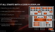
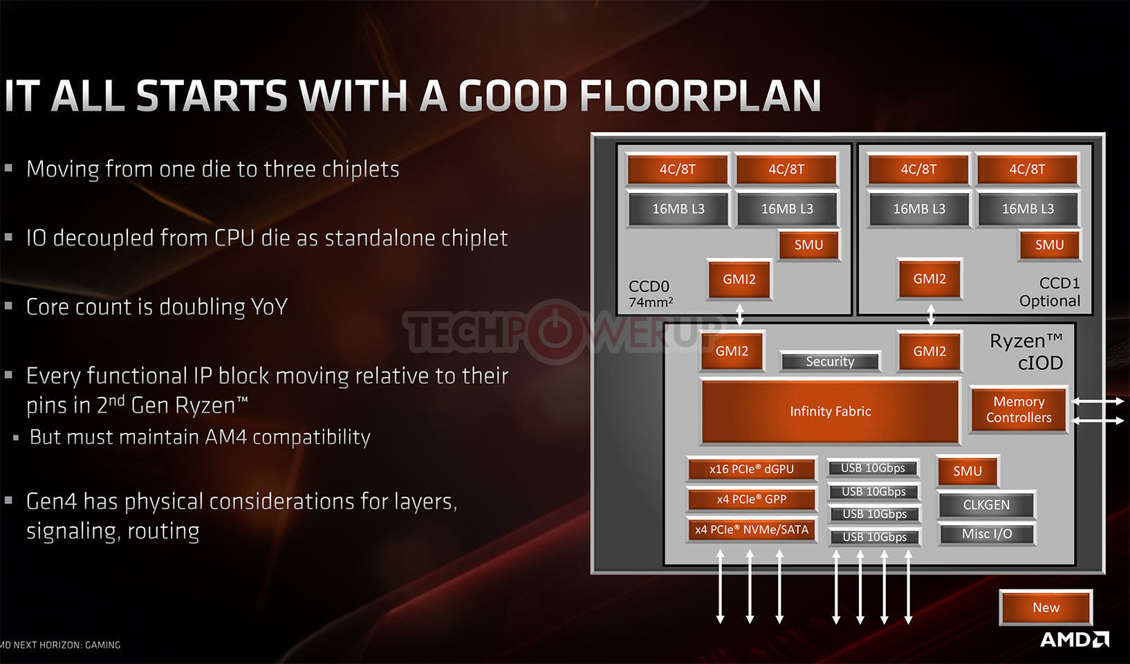
AMD Ryzen 3000 "Matisse" processors are multi-chip modules of two kinds of dies - one or two 7 nm 8-core "Zen 2" CPU chiplets, and an I/O controller die that packs the processor's dual-channel DDR4 memory controller, PCI-Express gen 4.0 root-complex, and an integrated southbridge that puts out some SoC I/O, such as two SATA 6 Gbps ports, four USB 3.1 Gen 2 ports, LPCIO (ISA), and SPI (for the UEFI BIOS ROM chip). It was earlier reported that while the Zen 2 CPU core chiplets are built on 7 nm process, the I/O controller is 14 nm. We have confirmation now that the I/O controller die is built on the more advanced 12 nm process, likely GlobalFoundries 12LP. This is the same process on which AMD builds its "Pinnacle Ridge" and "Polaris 30" chips. The 7 nm "Zen 2" CPU chiplets are made at TSMC.
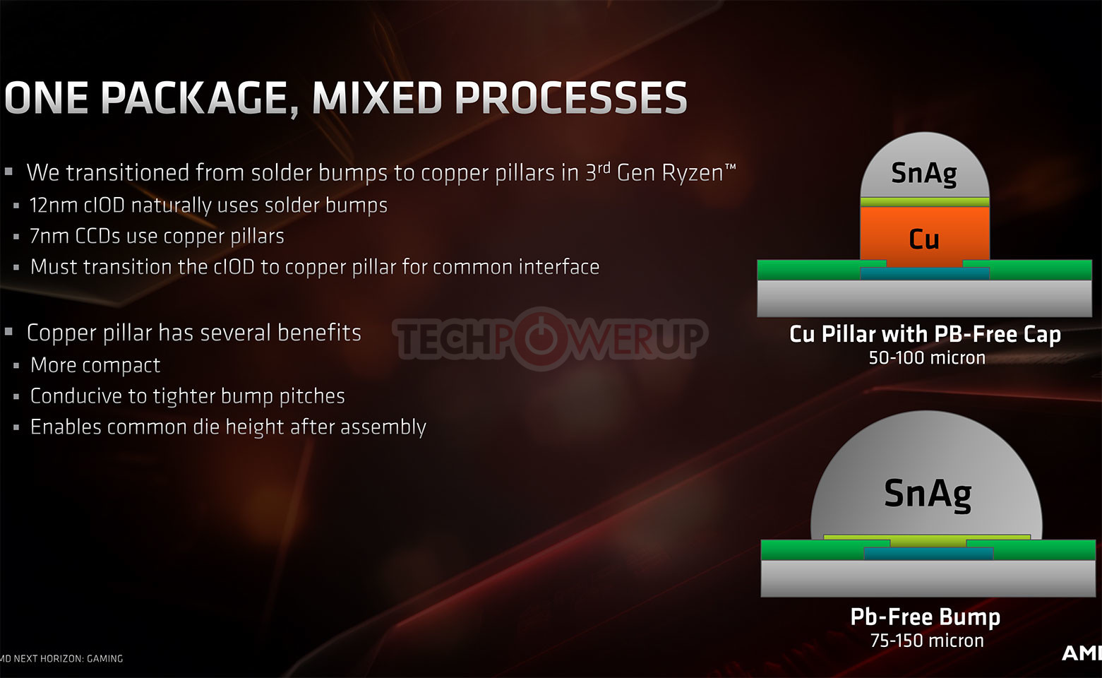
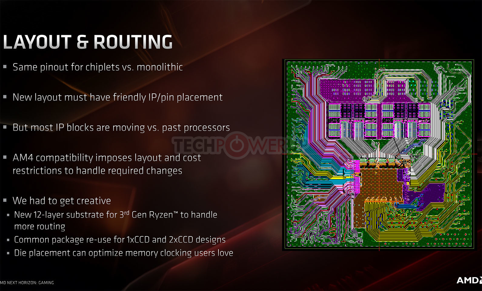
AMD also provided a fascinating technical insight to the making of the "Matisse" MCM, particularly getting three highly complex dies under the IHS of a mainstream-desktop processor package, and perfectly aligning the three for pin-compatibility with older generations of Ryzen AM4 processors that use monolithic dies, such as "Pinnacle Ridge" and "Raven Ridge." AMD innovated new copper-pillar 50µ bumps for the 8-core CPU chiplets, while leaving the I/O controller die with normal 75µ solder bumps. Unlike with its GPUs that need high-density wiring between the GPU die and HBM stacks, AMD could make do without a silicon interposer or TSVs (through-silicon-vias) to connect the three dies on "Matisse." The fiberglass substrate is now "fattened" up to 12 layers, to facilitate the inter-die wiring, as well as making sure every connection reaches the correct pin on the µPGA.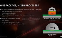
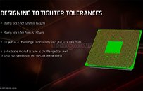

AMD also provided a fascinating technical insight to the making of the "Matisse" MCM, particularly getting three highly complex dies under the IHS of a mainstream-desktop processor package, and perfectly aligning the three for pin-compatibility with older generations of Ryzen AM4 processors that use monolithic dies, such as "Pinnacle Ridge" and "Raven Ridge." AMD innovated new copper-pillar 50µ bumps for the 8-core CPU chiplets, while leaving the I/O controller die with normal 75µ solder bumps. Unlike with its GPUs that need high-density wiring between the GPU die and HBM stacks, AMD could make do without a silicon interposer or TSVs (through-silicon-vias) to connect the three dies on "Matisse." The fiberglass substrate is now "fattened" up to 12 layers, to facilitate the inter-die wiring, as well as making sure every connection reaches the correct pin on the µPGA.

44 Comments on AMD Ryzen 3000 "Matisse" I/O Controller Die 12nm, Not 14nm
For me though 4 USB ports are enough. If there is a LAN and SATA contoller chip onboard, then there would be 2 more PCI-E x1 lanes free, 1 for sound card and 1 for an another SATA card or USB 3.0 card.
But true, it is easier if the Bx50 handles those I/O and storage devices.It's a little disappointing like they don't want me or others to buy their new Ryzen 3600 CPU. :(
There aren't many heatpipe coolers around these days,there's only one here. That'll change soon though.
geizhals.eu/?cat=coolchip&xf=10809_Chipsatz-K%FChler
if the chipset fan would be fixed, i.e 100% duty cycle all the time.
If you look at the A300/X300 boards, they technically don't have a chipset, just an I/O controller for legacy I/O, GPIO, I2C and a few things like that. So AMD has already done something along the lines of what you're asking for, it just didn't turn out to be very popular with the board makers, as their value add is close to zero.Well, maybe we'll see a resurgence of these kind of products...
edgeup.asus.com/2019/the-x570-motherboard-guide-ryzen-to-victory-with-pci-express-4-0/
I'm sad I will have to again despite it bringing me back memories of my youth.
Turn it around, define the use cases for that extra bandwidth right now. GPU - none. There is only storage, and any sane person has long since concluded that with simple SATA you've already eliminated most of the storage 'bottleneck' for I reckon over 90% of users.
What's really missing all these years was lane counts - never bandwidth. And even for that only a small group would feel inclined to get HEDT. Its not like that reality has suddenly changed. Even with the much faster storage available - speed is only useful if you can use it.
Regardless, PCIe 4.0 is irrelevant in the whole circus. AMD is killing it and it just keeps looking better for Zen. They have by far the most efficient use of chips and a product that has immense margin because of Intel's pricing strategy of the past decade.
In an ideal world, process sizes would actually tell the size of the smallest feature on a chip, but they dont in the real world. In this ideal world a 7nm gpu with identical features to a 12nm one would be 35% the size of the 12nm one. Which would mean that a 7nm 2070 would be roughly 156mm^2. The 5700xt is 251mm^2, or 56% the size of the 2070. Again we don't have all the info we need to know what kind of scaling we should be seeing, but I'm would bet that on equal footing the 5700xt would be bigger.
And "winning" should mean growing market share and making more money than Nvidia. AMD may grow market share, but I'm willing to bet that Nvidia will still have higher profits and a higher gross margin on each of there gpus sold.
www.techconsumerguide.com/nvidia-cuda-cores-vs-amd-stream-processor/Sure they will, they don't have the challenge of deciding what products/wafers should should go before who. I'm sure AMD/RTG scheduling all the 7nm start's they can get.
I guess I'm less attached to "greed is good".
AMD should probably aim for
- 3X more more instruction rate's over NAVI for it's successor
- 3X to 4X further lossless compression
- increase ROP's from 64 to 80
- improve the texture filter units by 0.5X
- improve texture mapping units by 0.5X to 1.5X (allowing for a better ratio of TFU's to TMU's)
- 3 CU resource pooling
- 7nm+ or node shrink
- more GDDR capacity hopefully I think by the time a successor arrives we could see more per chip GDDR6 capacity or a price reduction
- higher clocked GDDR
Bottom line I think AMD should really try to be more aggressive and further optimize it's efficiency of it's design and hopefully bump up frequency as well a bit. I don't think they need more stream processors right now, but rather need to improve the overall efficiency as a whole further to get more out of them. They also should aim to do some things to offer a few more GPU sku's to consumers at different price targets. I tend to think if they do that as well they might be able to even cut down chips to offer some good 2X or even 3X dual/triple GPU's as well based on PCIE 4.0 which good be good. I think if they could make the ROPs scale from 44/64/80 it would work well for just that type of thing and allowing better yields and binning options for AMD to offer to consumers.Those are my optimistic aggresive expectations of what AMD should try to aim towards for NAVI's successor if the R&D budget allows for it at least. They should really make some attempt to leap frog ahead a bit further especially as Nvidia will be shrinking down to a lower node for whatever comes after Turing or "SUPER" anyway since that sounds like more of a simply refresh and rebadge with a new bigger high end Super Titan sku added because what else would they name it instead 2080ti Super why!?!?Nvidia's GPU's are in general more granular in terms of workload management and thus power and efficiency. AMD needs to step it up more and it's not that AMD GPU's can't be efficient, but in order for a GPU like Vega 56/64 to compete with Nvidia's higher end and more diverse offers they have to stray more outside of power and efficiency so end up looking less efficient and more power hungry than they could be under more ideal circumstances with a better budget to design more complex and granular GPU's as Nvidia offers. It boils down to price segments and where they are marketed by both companies, but it's a more uphill battle for AMD given the R&D budget. The transition to 7nm was a smart call for AMD at least since it'll get cheaper over time along with yields and binning improvements. It should make for a easier transition to 7nm+ as well. Finer power gating would probably help out AMD a fair amount as well at improving TDP for load and idle and will become more important anyway at lower node sizes to reduce voltages and waste heat plus it's important for mobile which is a area for big room for growth for the company.
P.S. - I guess the is a 3rd option. Sell a lot of products with very high margins, the Apple way.
It more or less served the same function to connect the CPU to the memory and the fastest buses.
Which also connects to the SouthBridge for more Slower IO.
So in this case if the X570 really is just the Zen2 IO Die, it is a "NorthBridge" chip serving the function of a PCH / "SouthBridge".
My take on capitalism.
I say a true business isn't beholden to the stock price... They deliver a quality product at a price that enable's them to continuously move forward on products, quality and markets to maintain/secure their position and that of the employees who make them what they are.
Once you've worked a that kind of company you'll get it.
www.in-win.com/en/fans/mars/#product_download