Apr 1st, 2025 12:07 EDT
change timezone
Latest GPU Drivers
New Forum Posts
- WCG Daily Numbers (12822)
- RX 9000 series GPU Owners Club (93)
- Opened Thaiphoon then crash! (0)
- Folding Pie and Milestones!! (9454)
- Rare GPUs / Unreleased GPUs (2047)
- Help me pick a UPS (14)
- AMD RX 9070 XT & RX 9070 non-XT thread (OC, undervolt, benchmarks, ...) (76)
- What is the latest game you finished or 100% (16)
- TPU's Nostalgic Hardware Club (20147)
- best ram to buy for my usage and system specs? (3)
Popular Reviews
- DDR5 CUDIMM Explained & Benched - The New Memory Standard
- Sapphire Radeon RX 9070 XT Pulse Review
- ASRock Phantom Gaming B850 Riptide Wi-Fi Review - Amazing Price/Performance
- Palit GeForce RTX 5070 GamingPro OC Review
- SilverStone Lucid 04 Review
- Samsung 9100 Pro 2 TB Review - The Best Gen 5 SSD
- Sapphire Radeon RX 9070 XT Nitro+ Review - Beating NVIDIA
- Enermax REVOLUTION D.F. 12 850 W Review
- Assassin's Creed Shadows Performance Benchmark Review - 30 GPUs Compared
- AMD Ryzen 7 9800X3D Review - The Best Gaming Processor
Controversial News Posts
- MSI Doesn't Plan Radeon RX 9000 Series GPUs, Skips AMD RDNA 4 Generation Entirely (142)
- Microsoft Introduces Copilot for Gaming (124)
- AMD Radeon RX 9070 XT Reportedly Outperforms RTX 5080 Through Undervolting (119)
- NVIDIA Reportedly Prepares GeForce RTX 5060 and RTX 5060 Ti Unveil Tomorrow (115)
- Over 200,000 Sold Radeon RX 9070 and RX 9070 XT GPUs? AMD Says No Number was Given (100)
- NVIDIA GeForce RTX 5050, RTX 5060, and RTX 5060 Ti Specifications Leak (96)
- Retailers Anticipate Increased Radeon RX 9070 Series Prices, After Initial Shipments of "MSRP" Models (90)
- China Develops Domestic EUV Tool, ASML Monopoly in Trouble (88)
Wednesday, July 10th 2019

Intel Unveils New Tools in Its Advanced Chip Packaging Toolbox
What's New: This week at SEMICON West in San Francisco, Intel engineering leaders provided an update on Intel's advanced packaging capabilities and unveiled new building blocks, including innovative uses of EMIB and Foveros together and a new Omni-Directional Interconnect (ODI) technology. When combined with Intel's world-class process technologies, new packaging capabilities will unlock customer innovations and deliver the computing systems of tomorrow.
"Our vision is to develop leadership technology to connect chips and chiplets in a package to match the functionality of a monolithic system-on-chip. A heterogeneous approach gives our chip architects unprecedented flexibility to mix and match IP blocks and process technologies with various memory and I/O elements in new device form factors. Intel's vertically integrated structure provides an advantage in the era of heterogeneous integration, giving us an unmatched ability to co-optimize architecture, process and packaging to deliver leadership products." -Babak Sabi, Intel corporate vice president, Assembly and Test Technology Development.Why It's Important: Chip packaging has always played a critical - if under-recognized - role in the electronics supply chain. As the physical interface between the processor and the motherboard, the package provides a landing zone for a chip's electrical signals and power supply. As the electronics industry transitions to the data-centric era, advanced packaging will play a much larger role than it has in the past.
More than just the final step in the manufacturing process, packaging is becoming a catalyst for product innovation. Advanced packaging techniques allow integration of diverse computing engines across multiple process technologies with performance parameters similar to a single die, but with a platform scope that far exceeds the die-size limit of single-die integration. These technologies will improve product-level performance, power and area while enabling a complete rethinking of system architecture.
What are Intel's Updates: Intel is a leader in advanced packaging technology, with current offerings spanning both 2D and 3D approaches. At SEMICON West, Intel unveiled three new technologies that will open a new dimension in product architecture:
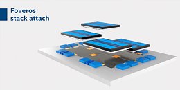
Co-EMIB: Intel's EMIB and Foveros technologies leverage high-density interconnects to enable high bandwidth at low power, with I/O density on par with or better than competitive approaches. The company's new Co-EMIB technology enables the linkage of even more computing performance and capability together. Co-EMIB allows for the interconnection of two or more Foveros elements with essentially the performance of a single chip. And designers can also connect analog, memory and other tiles with very high bandwidth and at very low power.
Collectively, these technologies are complementary tools in a powerful toolbox. When combined with Intel's process technologies, they form the underlying color palette for the creativity of its chip architects - giving them the freedom to dream up new products.
"Our vision is to develop leadership technology to connect chips and chiplets in a package to match the functionality of a monolithic system-on-chip. A heterogeneous approach gives our chip architects unprecedented flexibility to mix and match IP blocks and process technologies with various memory and I/O elements in new device form factors. Intel's vertically integrated structure provides an advantage in the era of heterogeneous integration, giving us an unmatched ability to co-optimize architecture, process and packaging to deliver leadership products." -Babak Sabi, Intel corporate vice president, Assembly and Test Technology Development.Why It's Important: Chip packaging has always played a critical - if under-recognized - role in the electronics supply chain. As the physical interface between the processor and the motherboard, the package provides a landing zone for a chip's electrical signals and power supply. As the electronics industry transitions to the data-centric era, advanced packaging will play a much larger role than it has in the past.
More than just the final step in the manufacturing process, packaging is becoming a catalyst for product innovation. Advanced packaging techniques allow integration of diverse computing engines across multiple process technologies with performance parameters similar to a single die, but with a platform scope that far exceeds the die-size limit of single-die integration. These technologies will improve product-level performance, power and area while enabling a complete rethinking of system architecture.
What are Intel's Updates: Intel is a leader in advanced packaging technology, with current offerings spanning both 2D and 3D approaches. At SEMICON West, Intel unveiled three new technologies that will open a new dimension in product architecture:
Co-EMIB: Intel's EMIB and Foveros technologies leverage high-density interconnects to enable high bandwidth at low power, with I/O density on par with or better than competitive approaches. The company's new Co-EMIB technology enables the linkage of even more computing performance and capability together. Co-EMIB allows for the interconnection of two or more Foveros elements with essentially the performance of a single chip. And designers can also connect analog, memory and other tiles with very high bandwidth and at very low power.
ODI: Intel's new Omni-Directional Interconnect provides even greater flexibility for communication among chiplets in a package. The top chip can communicate horizontally with other chiplets, similar to EMIB. It can also communicate vertically with through-silicon vias (TSVs) in the base die below, similar to Foveros. And ODI leverages large vertical vias to allow power delivery to the top die directly from the package substrate. Much larger than traditional TSVs, the large vias have lower resistance, providing more robust power delivery simultaneously with higher bandwidth and lower latency enabled through stacking. At the same time, this approach reduces the number of TSVs required in the base die, freeing up more area for active transistors and optimizing die size.
MDIO: Building upon its Advanced Interface Bus (AIB) PHY level interconnect, Intel disclosed a new die-to-die interface called MDIO. The technology enables a modular approach to system design with a library of chiplet intellectual property blocks. MDIO provides better power efficiency and more than double the pin speed and bandwidth density offered by AIB.
Collectively, these technologies are complementary tools in a powerful toolbox. When combined with Intel's process technologies, they form the underlying color palette for the creativity of its chip architects - giving them the freedom to dream up new products.
Apr 1st, 2025 12:07 EDT
change timezone
Latest GPU Drivers
New Forum Posts
- WCG Daily Numbers (12822)
- RX 9000 series GPU Owners Club (93)
- Opened Thaiphoon then crash! (0)
- Folding Pie and Milestones!! (9454)
- Rare GPUs / Unreleased GPUs (2047)
- Help me pick a UPS (14)
- AMD RX 9070 XT & RX 9070 non-XT thread (OC, undervolt, benchmarks, ...) (76)
- What is the latest game you finished or 100% (16)
- TPU's Nostalgic Hardware Club (20147)
- best ram to buy for my usage and system specs? (3)
Popular Reviews
- DDR5 CUDIMM Explained & Benched - The New Memory Standard
- Sapphire Radeon RX 9070 XT Pulse Review
- ASRock Phantom Gaming B850 Riptide Wi-Fi Review - Amazing Price/Performance
- Palit GeForce RTX 5070 GamingPro OC Review
- SilverStone Lucid 04 Review
- Samsung 9100 Pro 2 TB Review - The Best Gen 5 SSD
- Sapphire Radeon RX 9070 XT Nitro+ Review - Beating NVIDIA
- Enermax REVOLUTION D.F. 12 850 W Review
- Assassin's Creed Shadows Performance Benchmark Review - 30 GPUs Compared
- AMD Ryzen 7 9800X3D Review - The Best Gaming Processor
Controversial News Posts
- MSI Doesn't Plan Radeon RX 9000 Series GPUs, Skips AMD RDNA 4 Generation Entirely (142)
- Microsoft Introduces Copilot for Gaming (124)
- AMD Radeon RX 9070 XT Reportedly Outperforms RTX 5080 Through Undervolting (119)
- NVIDIA Reportedly Prepares GeForce RTX 5060 and RTX 5060 Ti Unveil Tomorrow (115)
- Over 200,000 Sold Radeon RX 9070 and RX 9070 XT GPUs? AMD Says No Number was Given (100)
- NVIDIA GeForce RTX 5050, RTX 5060, and RTX 5060 Ti Specifications Leak (96)
- Retailers Anticipate Increased Radeon RX 9070 Series Prices, After Initial Shipments of "MSRP" Models (90)
- China Develops Domestic EUV Tool, ASML Monopoly in Trouble (88)


7 Comments on Intel Unveils New Tools in Its Advanced Chip Packaging Toolbox
well this article was DoA it seems
Intel says: we found some glue!
:D
But Intel can show off renders and non-functional "chips", but all I have to do is look left to the desktop sitting on my desk, and see AMD's advanced packaging living and breathing in real life, in a real application that works flawlessly...
uhmm i have one.
Shintel says: uhh count to ten? 2, 4, 6, 8, 8, 8. Get it? they can't count more than 8 dude
hahahaha. really wonder how Intel still exists sometimes you know