Thursday, May 14th 2020

NVIDIA GA100 Scalar Processor Specs Sheet Released
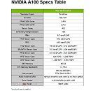
NVIDIA today unveiled the GTC 2020, online event, and the centerpiece of it all is the GA100 scalar processor GPU, which debuts the "Ampere" graphics architecture. Sifting through a mountain of content, we finally found the slide that matters the most - the specifications sheet of GA100. The GA100 is a multi-chip module that has the 7 nm GPU die at the center, and six HBM2E memory stacks at its either side. The GPU die is built on the TSMC N7P 7 nm silicon fabrication process, measures 826 mm², and packing an unfathomable 54 billion transistors - and we're not even counting the transistors on the HBM2E stacks of the interposer.
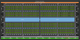
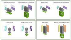
The GA100 packs 6,912 FP32 CUDA cores, and independent 3,456 FP64 (double-precision) CUDA cores. It has 432 third-generation tensor cores that have FP64 capability. The three are spread across a gargantuan 108 streaming multiprocessors. The GPU has 40 GB of total memory, across a 6144-bit wide HBM2E memory interface, and 1.6 TB/s total memory bandwidth. It has two interconnects: a PCI-Express 4.0 x16 (64 GB/s), and an NVLink interconnect (600 GB/s). Compute throughput values are mind-blowing: 19.5 TFLOPs classic FP32, 9.7 TFLOPs classic FP64, and 19.5 TFLOPs tensor cores; TF32 156 TFLOPs single-precision (312 TFLOPs with neural net sparsity enabled); 312 TFLOPs BFLOAT16 throughout (doubled with sparsity enabled); 312 TFLOPs FP16; 624 TOPs INT8, and 1,248 TOPS INT4. The GPU has a typical power draw of 400 W in the SXM form-factor. We also found the architecture diagram that reveals GA100 to be two almost-independent GPUs placed on a single slab of silicon. We also have our first view of the "Ampere" streaming multiprocessor with its FP32 and FP64 CUDA cores, and 3rd gen tensor cores. The GeForce version of this SM could feature 2nd gen RT cores.
The GA100 packs 6,912 FP32 CUDA cores, and independent 3,456 FP64 (double-precision) CUDA cores. It has 432 third-generation tensor cores that have FP64 capability. The three are spread across a gargantuan 108 streaming multiprocessors. The GPU has 40 GB of total memory, across a 6144-bit wide HBM2E memory interface, and 1.6 TB/s total memory bandwidth. It has two interconnects: a PCI-Express 4.0 x16 (64 GB/s), and an NVLink interconnect (600 GB/s). Compute throughput values are mind-blowing: 19.5 TFLOPs classic FP32, 9.7 TFLOPs classic FP64, and 19.5 TFLOPs tensor cores; TF32 156 TFLOPs single-precision (312 TFLOPs with neural net sparsity enabled); 312 TFLOPs BFLOAT16 throughout (doubled with sparsity enabled); 312 TFLOPs FP16; 624 TOPs INT8, and 1,248 TOPS INT4. The GPU has a typical power draw of 400 W in the SXM form-factor. We also found the architecture diagram that reveals GA100 to be two almost-independent GPUs placed on a single slab of silicon. We also have our first view of the "Ampere" streaming multiprocessor with its FP32 and FP64 CUDA cores, and 3rd gen tensor cores. The GeForce version of this SM could feature 2nd gen RT cores.


101 Comments on NVIDIA GA100 Scalar Processor Specs Sheet Released
OK, we're making shit up ?
Pure FP64 performance sits at 9.7 TFLOPS, Tensor FP64 at 19.5. They are not interchangeable you blithering ... genius. If you write a kernel that adds two FP64 vectors, you'll get 9.7 TFLOPS not 19.5.
What you are talking about applies to the TF32 format which doesn't require any change in code, there is no "TF64" format with reduced precision. However that doesn't apply to any workload either. THEY ARE DIFFERENT EXECUTION UNITS FOR DIFFERENT THINGS. One does scalar FMAs (FP64), one does the two dimensional equivalent of FMAs (Tensor FP64).
It just get's better and better with you, I am getting tired of lecturing you and making fun of you along the way. It's time to stop, the longer we're at it the lesser your knowledge on the subject gets.
Furthermore this means you didn't even read my post before hitting the reply button . If Tensor Cores were taking so much space how do you explain that GA 100 die size has increased compared to GV 100 despite Tensor Core count having significantly decreased at the same time ???
devblogs.nvidia.com/nvidia-ampere-architecture-in-depth/I hope this was educational for you.
Tensor operations
Tensor operations
This is a a tensor operation :
Those "FP64" units you see in the SM diagram don't do tensor operation, they just do scalar ops. Different units, for different workloads. "FP64 workload" means scalar, not tensor. "Tensor FP64" means tensors not scalar. Even a high school senior would understand this.
Tensor FP64 != FP64. A tensor operation is a mixed precision computation, you can't call it "FP64 workload" because it's not pure 64 bit floating point all throughout the computation. You can't do arbitrary computations with those cores like you can with the scalar FP64 ones either.
Let me ask you this, if they mean the same thing why mention two separate figures, 9.7 and 19.5 ? What's the 9.7 for ? Cupcake operations ?
See, one is just "Peak FP64" and the other very clearly says "Peak FP64 Tensor Core". Meaning that big rectangle in the SM diagram. Different units for different workloads.
I am convinced you can't be educated, you are missing both the will and the capacity to understand this. I find it bewildering you can literally post something that proves you wrong and still not admit it. You are something else, I really hope they're paying you for this intellectual suicide.
I have all day by the way, I am your nemesis.
YOU CAN'T OBTAIN THAT 19.5 TFLOP RATING WITH THESE UNITS.Yep, those are tensor cores which do tensor operations not scalar FP64 FMAs, IEEE compliant just means the elements within the data structure meets those standards, the computation is not your standard FMA. Those are used for tensor workloads not pure FP64 workloads, get it now you highly intelligent individual* ?.
* may be subject to sarcasm
Different units for different workloads. You can't add two FP64 vectors with Tensor Cores because you'd get a wrong answer, you can however implement tensor operation with FP64 units.
Here we go again :
There are 8*4=32 FP64 units in each SM, fucking count them, use your fingers like in preschool. Each does 1 FMA meaning 64 in total, 64*108*1400 = 9 676 800 FLOPS.
WHEN THEY SAY 128 FP64 OPERATIONS PER CLOCK IN ONE SM THEY ARE ALSO COUNTING THE TENSOR CORES ! But those are different units that do different things, they are mixing together different things in order to fool the likes you. They've done a good job.
Let me get this straight, are you suggesting Nvidia wrote that "Peak FP64" figure ... by mistake ?
:roll:
It's like you're making up your own reality.
The new double precision matrix multiply-add instruction on A100 replaces eight DFMA instructions on V100, DFMA: is Double Percision Fused Multiply Add. So each matrix multiply-add instruction now replaces 8 FP64 fused multiply-add instructions. 1 replaces 8.Where do you think those 128 FP64 operations come from?Why are you insisting on ignoring everything NVIDIA is saying in their whitepaper? Ego much?
FP64 units can only do 64 ops per SM per clock cycle. That provides your FP64 throughput which is different from FP64 tensor throughput. They are not the same, you can't quantify them all in one group and Nvidia makes this very clear by providing two figures : 9.7 TFLOPS of FP64 and 19.5 TFLOPS of Tensor FP64. It seems like it's you who can't read anything from their white paper.
LEARN to read the whitepaper.Your ego is creaking under the immense pressure of the massive amount of BS inside. You can't admit you were wrong, you are a bad loser.
IEEE compliant just means the elements in the data structure adheres to the FP64 standard. That data structure isn't scalar, it's a matrix (technically a vector).
Tensor core != FP64 core.They've simply increased the amount of units.
Can you branch within in a tensor like you can with scalar CUDA code ? No, you can't.
And you didn't answer LOL, which units?
Tensor
Tensor
Do you just like, filter out the words you don't like ? Show me where it says this : "scalar code can now be accelerated by tensor operations". Stop spamming this shit which I've explained thoroughly that it has nothing to do with scalar code. Nvidia provides two performance metrics, one for scalar FP64 performance (9.7 TFLOPS) and one for FP64 tensor ops (19.5 TFLOPS) because they are different types of operations handled by different units.Lawl.
Let's make a deal, I tell you which units when you tell me why does Nvidia provide two different metrics for what you claim is the same thing because I kept asking this as well and you didn't answer me. OK ?
For example, V100 lacks INT8 hardware, it can be done on software on the CUDA cores, but A100 can do INT8 with Tensor cores at a massive speed increase, and it can do 20X the amount of V100. Likewise with FP16 code, it can be done with CUDA cores, but the Tensor cores can do them at much faster speeds in V100 and A100.
NVIDIA reports the peak performance for each unit, but that's irrelevant, because at the end of the day, the A100 can do 2.5X the FP64 output of V100, which was the original point that went over your head.
Do you understand how nonsensical this is ?Fixed itIt's only irrelevant in your head. Imagine thinking that a billion dollar company trying to sell millions of dollars worth of equipment would just write a bunch of worthless crap in their specifications. :roll:
They are peak performance metrics for two separate things. You can't use Tensor core to run scalar code on them, it simply doesn't work like that. The PF64 units can do branching, masking, execute complex mathematical functions, bit wise instructions, etc. Tensor cores can't do any of those things, they just do one single bloody computation : A * B + D. Unless you show me where this is explicitly mentioned and explained you are straight up delusional and making shit up. You don't have the slightest clue how these things even work, otherwise it would be painfully obvious to you how dumb what you're saying is.
Anyway to answer your question, the throughput of tensor operations is higher because obviously the throughput of Tensor Cores is higher and there are more SMs. Tensor operations use the tensor units. It's like I am explaining this to a 5 year old.
In the end, NVIDIA clearly mentions 3 things:
Tenor cores are now compliant with accelerating accelerate IEEE-compliant FP64 computations
Each FP64 matrix multiply add op now replaces 8 FMA FP64 operation
Meaning each SM is now capable of 128 FP64 op per clock which achieves 2.5X the throughput of V100
So A100 is 2.5X the V100 FP64 througput.
Case closed.
You are so wrong, stubborn and unintelligent, you've exceed all my expectations from past discussions with you. Anyway I thought you "rested" your case many comments ago, why are you still here ?
EgO mUcH ? Remember if you don't want to deal with me anymore then don't tell I'm wrong when I'm not. It's that simple, otherwise we can go on forever, I have all day as I said.