Thursday, May 14th 2020

NVIDIA GA100 Scalar Processor Specs Sheet Released
NVIDIA today unveiled the GTC 2020, online event, and the centerpiece of it all is the GA100 scalar processor GPU, which debuts the "Ampere" graphics architecture. Sifting through a mountain of content, we finally found the slide that matters the most - the specifications sheet of GA100. The GA100 is a multi-chip module that has the 7 nm GPU die at the center, and six HBM2E memory stacks at its either side. The GPU die is built on the TSMC N7P 7 nm silicon fabrication process, measures 826 mm², and packing an unfathomable 54 billion transistors - and we're not even counting the transistors on the HBM2E stacks of the interposer.
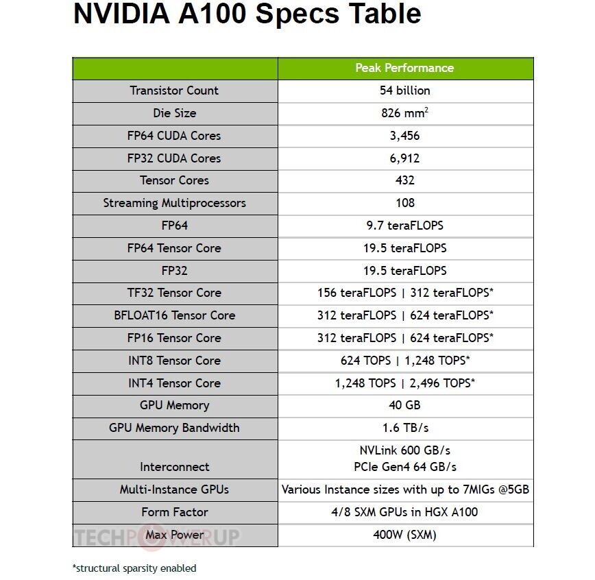
The GA100 packs 6,912 FP32 CUDA cores, and independent 3,456 FP64 (double-precision) CUDA cores. It has 432 third-generation tensor cores that have FP64 capability. The three are spread across a gargantuan 108 streaming multiprocessors. The GPU has 40 GB of total memory, across a 6144-bit wide HBM2E memory interface, and 1.6 TB/s total memory bandwidth. It has two interconnects: a PCI-Express 4.0 x16 (64 GB/s), and an NVLink interconnect (600 GB/s). Compute throughput values are mind-blowing: 19.5 TFLOPs classic FP32, 9.7 TFLOPs classic FP64, and 19.5 TFLOPs tensor cores; TF32 156 TFLOPs single-precision (312 TFLOPs with neural net sparsity enabled); 312 TFLOPs BFLOAT16 throughout (doubled with sparsity enabled); 312 TFLOPs FP16; 624 TOPs INT8, and 1,248 TOPS INT4. The GPU has a typical power draw of 400 W in the SXM form-factor. We also found the architecture diagram that reveals GA100 to be two almost-independent GPUs placed on a single slab of silicon. We also have our first view of the "Ampere" streaming multiprocessor with its FP32 and FP64 CUDA cores, and 3rd gen tensor cores. The GeForce version of this SM could feature 2nd gen RT cores.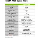
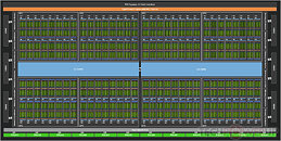
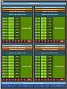
The GA100 packs 6,912 FP32 CUDA cores, and independent 3,456 FP64 (double-precision) CUDA cores. It has 432 third-generation tensor cores that have FP64 capability. The three are spread across a gargantuan 108 streaming multiprocessors. The GPU has 40 GB of total memory, across a 6144-bit wide HBM2E memory interface, and 1.6 TB/s total memory bandwidth. It has two interconnects: a PCI-Express 4.0 x16 (64 GB/s), and an NVLink interconnect (600 GB/s). Compute throughput values are mind-blowing: 19.5 TFLOPs classic FP32, 9.7 TFLOPs classic FP64, and 19.5 TFLOPs tensor cores; TF32 156 TFLOPs single-precision (312 TFLOPs with neural net sparsity enabled); 312 TFLOPs BFLOAT16 throughout (doubled with sparsity enabled); 312 TFLOPs FP16; 624 TOPs INT8, and 1,248 TOPS INT4. The GPU has a typical power draw of 400 W in the SXM form-factor. We also found the architecture diagram that reveals GA100 to be two almost-independent GPUs placed on a single slab of silicon. We also have our first view of the "Ampere" streaming multiprocessor with its FP32 and FP64 CUDA cores, and 3rd gen tensor cores. The GeForce version of this SM could feature 2nd gen RT cores.


101 Comments on NVIDIA GA100 Scalar Processor Specs Sheet Released
But there won't be 2 different 100s, technically that is what the 102 is.
Got ya.
From this :
To this:
To be honest this is borderline Thermi 2.0, a great compute architecture that can barley be implemented in actual silicon due to power and yields. These aren't exactly Nvidia's brightest hours in terms of chip design, it seems like they bit more than what they could chew, the chip was probably cut down in a last minute decision.
Suffice to say I doubt we'll see the full 8192 shaders in any GPU this generation, I doubt they could realistically fit that in a 250W power envelope and it seems like GA100 runs at 1.4 Ghz, no change from Volta nor from Turing probably. Let's see 35% more shaders than Volta but 60% more power and same clocks. It's not shaping up to be the "50% more efficient and 50% faster per SM" some hoped for.
There is no real correlation between die size increase and fixed function as the latter eats relatively very low die space , more likely than not the higher die size in Turing is explained by the fact that it has more SMs .
This is further backed up by GA100 which has increased dies size compared to GV100 ( 826mm^2 vs 815mm^2 ) but significantly lower TensorCore count ( 432 vs 640 ) . So it is pretty obvious that fixed function hardware is not responsible for the die size expansion !This was exactly my point , the only tangible argument that justifies higher prices for Turing ( other than the increased silicon size ) is because the lack of competition allows them to do so .
The A100 packs 54 billion transistors, 2.5 times as much as a V100, and those transistors aren't there for nothing.
You can't just compare SM counts and base stupid assumptions upon that. The A100 is clearly a much more efficient solution for what it's been designed for.
Let's face reality, they couldn't enable the entire chip because of power constraints. Making a chip like that isn't desirable, it's painfully obvious they've missed their target by miles.
So, based on your logic the Vega 56 is a more efficient GPU than AMD's latest and greatest 5700 XT, because it has more TFLOPS and much more compute units, and consumes similar amounts of power, right?
Based on the density figures, I think Nvidia is using TSMC's high-density version of their 7nm node, not the high-performance one, and that was not the case with previous generations.
They could just use the normal high performance version and scale up the GV100 chip, but they clearly needed more density for their design goals.
What I'm saying is that you have to see how the chip performs in applications that actully matter and base efficiency figures upon that, not just some raw numbers.
Because you do know how to design a GPU, right ? Sorry your GPU architect badge must have fallen off.Nope, that's based on your logic. Your understanding of what I said was obviously severely limited.
First of all Vega 56 uses more power, and runs at lower clocks. A legendary GPU architect like yourself would know that a larger processor at lower clocks runs more efficiently because shaders scale relativity linearly with power whereas a change in clocks incurs a change in voltage which isn't linear. In other words if let's say we have a GPU with N/2 shaders at 2 Ghz it will generally consume more power than a GPU with N shaders at 1 Ghz.
Let's compile that with how Navi works : RX 5700XT runs at a considerably higher voltages and clocks and has way less shaders and yet it generates a similar amount of FP32 compute with less power. It's obviously way more efficient architecturally, but as I already mentioned I am sure a world renowned GPU architect as yourself knew all that.
On the other hand, Volta and Ampere run at pretty much the same frequency and likely similar voltages since TSMC's 7nm doesn't seem to change that in any significant manner (in fact all 7nm CPU/GPU up until know seem to run at the same or even higher voltages), GA100 has 20% more shaders compared to V100 but also consumes 60% more power. It doesn't take much to see that efficiency isn't that great. It's not that hard to infer these things, don't overestimate their complexity.
Yes, I am sure when you factor in Nvidia's novel floating point formats it looks great, but if you look just at FP32, it's doesn't look great. It's rather mediocre. Do you not find it strange that our boy Jensen never once mentioned FP32 performance ?
I never said I knew how to design it better, stop projecting made up staff onto me. I said it was obvious they failed to do what they originally set out to do, hence why a considerable porton of the chip is fused off. They've done it in the past too.
Jensen wasn't baking it in his oven, he used them to heat his oven.
nvidia/comments/99r2x3caly-technologies.com/die-yield-calculator/
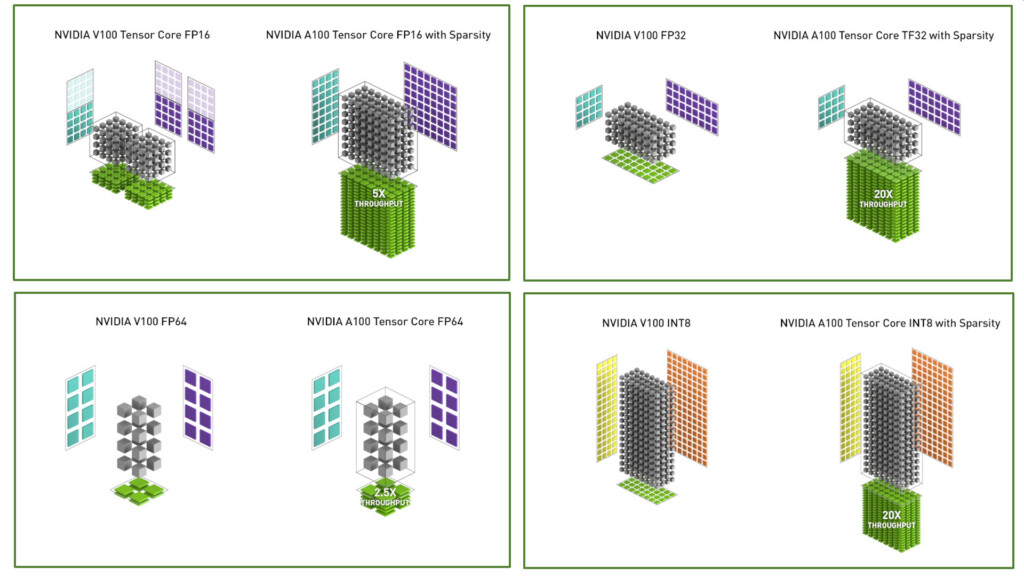
Alright A100 provides 156 TF FP32 compared to only 15 TF in V100. That alone is 10X increase in FP32 compute power without the need to change any code. They can extend that lead to 20X through sparse network optimizations to 312 TF of FP32 without code change.
In FP16 the increase is also 2.5X in non optimzied code, and 6X in optimized code, same for INT8 and INT4 numbers, so A100 is really several orders of magnitude faster than V100 in any AI workload.
Also the 400w of power consumption is nothing relative to the size of this monster, you have 40GB of HBM2, loads of NVLink connections, loads of tensor cores that take up die area, heat and power, the chip is also cut down (which means lost power consumption), also the trend in data centers and AI is to open power consumption up to allow for more comfortable performance, V100 reached 350W in it's second iteration and 450W in its third iteration.
You seem to lack any ounce of data center experience, so I just suggest you stick to the of analysis consumer GPUs. This isn't your area.
9.7 / 7.8 = 1.24X (FP64)
Or maybe Jensen did a good job deceiving the less tech literate with their fine print by mixing together FP64 with FP64 TF.
Nice paint skills by the way.
Is so typical of nvidia.They cheaped out, instead of offering 6 modules of 8 gb, for a total of 48 gb, they wen for higher margins. Will offer a better improved version with full 48 gb memory, 25 mhz more, on core and memory, for 5000 dollar more. Dunn worry about it.
Is so typical of nvidia.
FP64 from Tensor cores is 19.5TF. Which is a 2.5X increase over V100. FP64 from CUDA cores is 9.7TF. If you can use both at the same time you will get about 30TF of FP64 for AI actually.It's much more meaningful than the ignorant job you did, analysing regular FP32/FP64 in an AI GPU. Talk about an extreme case of stuff that are way over your head.
You wrote "FP64 workloads", you genius. That's pure FP64 not tensor ops, you're clueless and stubborn.
Sheesh.