Thursday, May 14th 2020

NVIDIA GA100 Scalar Processor Specs Sheet Released

NVIDIA today unveiled the GTC 2020, online event, and the centerpiece of it all is the GA100 scalar processor GPU, which debuts the "Ampere" graphics architecture. Sifting through a mountain of content, we finally found the slide that matters the most - the specifications sheet of GA100. The GA100 is a multi-chip module that has the 7 nm GPU die at the center, and six HBM2E memory stacks at its either side. The GPU die is built on the TSMC N7P 7 nm silicon fabrication process, measures 826 mm², and packing an unfathomable 54 billion transistors - and we're not even counting the transistors on the HBM2E stacks of the interposer.

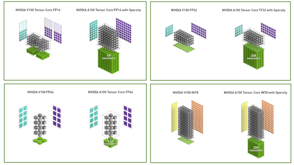
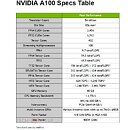
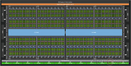
The GA100 packs 6,912 FP32 CUDA cores, and independent 3,456 FP64 (double-precision) CUDA cores. It has 432 third-generation tensor cores that have FP64 capability. The three are spread across a gargantuan 108 streaming multiprocessors. The GPU has 40 GB of total memory, across a 6144-bit wide HBM2E memory interface, and 1.6 TB/s total memory bandwidth. It has two interconnects: a PCI-Express 4.0 x16 (64 GB/s), and an NVLink interconnect (600 GB/s). Compute throughput values are mind-blowing: 19.5 TFLOPs classic FP32, 9.7 TFLOPs classic FP64, and 19.5 TFLOPs tensor cores; TF32 156 TFLOPs single-precision (312 TFLOPs with neural net sparsity enabled); 312 TFLOPs BFLOAT16 throughout (doubled with sparsity enabled); 312 TFLOPs FP16; 624 TOPs INT8, and 1,248 TOPS INT4. The GPU has a typical power draw of 400 W in the SXM form-factor. We also found the architecture diagram that reveals GA100 to be two almost-independent GPUs placed on a single slab of silicon. We also have our first view of the "Ampere" streaming multiprocessor with its FP32 and FP64 CUDA cores, and 3rd gen tensor cores. The GeForce version of this SM could feature 2nd gen RT cores.
Add your own comment

101 Comments on NVIDIA GA100 Scalar Processor Specs Sheet Released

#76
dyonoctis
At the end of the day, the only thing that matter is that tensor cores/FP64 are not going to benefits games that don't use DLSS. Ampere for gaming is probably going to be different.
Posted on Reply
#77
MuhammedAbdo
Vya Domusdifferent performance metrics for the two
NVIDIA is directly comparing the V100 FP64 output to the A100 FP64 2.5X output, which means they are directly comparable.
Vya DomusFixed it. Tensor cores do tensor operations. That's why they are called tensor cores.
Adding imaginary stuff out of your ass isn't fixing anything, it just proves how fragile and flawed your logic is, that you resorted to adding stuff that isn't there to convince yourself you are still right! I pity you.
Posted on Reply
#78
Dante Uchiha
RH92Dude are you seriously trying to back up your argument with some random Reddit post ( which is not even close to be accurate to begin with ) ??? Come on now i though you were serious !


For starter stop repeating the same misinformation that has been debunked , the SM diagram is just a general representation of the architecture and represents in no way the physical size of individual segments , this is public knowledge !

Furthermore this means you didn't even read my post before hitting the reply button . If Tensor Cores were taking so much space how do you explain that GA 100 die size has increased compared to GV 100 despite Tensor Core count having significantly decreased at the same time ???
That post on reddit is not far from reality.

You're comparing orange to apples. You can't use different architectures as basis... Do I really need to explain the density difference between Volta at 12nm (24mT/mm²) vs Ampere at 7nm (65mT/mm²) ?
Posted on Reply
#79
Vya Domus
MuhammedAbdoNVIDIA is directly comparing the V100 FP64 output to the A100 FP64 2.5X output, which means they are directly comparable.
Nope, they are comparing the FP64 throughput separately from the FP64 tensor throughput because they are different things.
MuhammedAbdoAdding imaginary stuff out of your ass isn't fixing anything
Gaslighting, classic. You've made shit up such as tensor cores running scalar code and claiming that Nvidia said so when they didn't. You claim all metrics are actually the same thing and the people at Nvidia are just a bunch of idiots wasting their time writing irrelevant shit. You live in a parallel world buddy, I think your condition is called cognitive dissonance. For your own mental health, go check a doctor.

I pity you that you pity me :).

But you didn't answer, what are you still doing here ? Let the case rest buddy, you said it's settled. Feeling insecure about the nonsense that you wrote ?
Posted on Reply
#80
dyonoctis
To be fair, nvidia seems to have made a few typo in one of their slides where they forgot to add "TC" next to to V100, wich make it looks like they are pitting FP32/64 TC against classic FP32/64.
Posted on Reply
#81
MuhammedAbdo
Vya DomusYou've made shit up such as tensor cores running scalar code and claiming that Nvidia said so when they didn't.
How many phrases should I quote from the whitepaper?

Tenor cores are now compliant with accelerating IEEE-compliant FP64 computations
Each FP64 matrix multiply add op now replaces 8 FMA FP64 operation
Meaning each SM is now capable of 128 FP64 op per clock which achieves 2.5X the throughput of V100
Vya DomusBut you didn't answer, what are you still doing here ? Let the case rest buddy, you said it's settled. Feeling insecure about the nonsense that you wrote ?
I am here simply to educate.
dyonoctisTo be fair, nvidia seems to have made a few typo in one of their slides where they forgot to add "TC" next to to V100, wich make it looks like they are pitting FP32/64 TC against classic FP32/64.
There is no typo, they did the same on this official slide:

Posted on Reply
#82
Vya Domus
MuhammedAbdoHow many phrases should I quote from the whitepaper?
It's not a whitepaper, stop saying this. You're not citing some sort of scientific paper buddy, it's a damn blog post on their website. And your "whitepaper", by the way, agrees with me not you.
MuhammedAbdoTenor cores are now compliant with accelerating IEEE-compliant FP64 computations
It doesn't mean anything if they are compliant they are distinct units different from the normal FP64 units as the SM diagram clearly shows because they do different computations.
MuhammedAbdoMeaning each SM is now capable of 128 FP64 op per clock which achieves 2.5X the tensor FP64 throughput of V100
Fixed it.

Don't worry, just as you can spam the same incorrect statements a million times I can also correct you every time.
MuhammedAbdoI am here simply to educate.
I did not need or request your worthless education. I mean for one thing you are absolutely clueless, who do you think you are, a scholar ? On some random tech forum wasting your time spamming the same shit over and over ?

Wake up to the real world buddy, you ain't educating anyone. :roll:
Posted on Reply
#83
MuhammedAbdo
Vya DomusIt doesn't mean anything if they are compliant they are distinct units different from the normal FP64 units as the SM diagram clearly shows because they do different computations.
Figuring out the double precision floating point performance boost moving from Volta to Ampere is easy enough. Paresh Kharya, director of product management for datacenter and cloud platforms, said in a prebriefing ahead of the keynote address by Nvidia co-founder and chief executive officer Jensen Huang announcing Ampere that peak FP64 performance for Ampere was 19.5 teraflops (using Tensor Cores), 2.5X larger than for Volta. So you might be thinking that the FP64 unit counts scaled with the increase of the transistor density, more or less. But actually, the performance of the raw FP64 units in the Ampere GPU only hits 9.7 teraflops, half the amount running through the Tensor Cores (which did not support 64-bit processing in Volta.)
www.nextplatform.com/2020/05/14/nvidia-unifies-ai-compute-with-ampere-gpu/

Sucks to be you I guess.

As already mentioned, the A100 is 2.5x more efficient in accelerating FP64 workloads compared to the V100. This was achieved by replacing the traditional DFMA instructions with FP64 based matrix multiply-add. This reduces the scheduling overhead and shared memory bandwidth requirement by cutting down on instruction fetches.
www.hardwaretimes.com/nvidia-ampere-architectural-analysis-a-look-at-the-a100-tensor-core-gpu/amp/

With FP64 and other new features, the A100 GPUs based on the NVIDIA Ampere architecture become a flexible platform for simulations, as well as AI inference and training — the entire workflow for modern HPC. That capability will drive developers to migrate simulation codes to the A100.

Users can call new CUDA-X libraries to access FP64 acceleration in the A100. Under the hood, these GPUs are packed with third-generation Tensor Cores that support DMMA, a new mode that accelerates double-precision matrix multiply-accumulate operations.

A single DMMA job uses one computer instruction to replace eight traditional FP64 instructions. As a result, the A100 crunches FP64 math faster than other chips with less work, saving not only time and power but precious memory and I/O bandwidth as well.

We refer to this new capability as Double-Precision Tensor Cores.

agenparl.eu/double-precision-tensor-cores-speed-high-performance-computing/

Ouch, suck for you again!
Posted on Reply
#84
Vya Domus
MuhammedAbdoParesh Kharya, director of product management for datacenter and cloud platforms, said in a prebriefing ahead of the keynote address by Nvidia co-founder and chief executive officer Jensen Huang announcing Ampere that peak FP64 performance for Ampere was 19.5 teraflops (using Tensor Cores), 2.5X larger than for Volta. So you might be thinking that the FP64 unit counts scaled with the increase of the transistor density, more or less. But actually, the performance of the raw FP64 units in the Ampere GPU only hits 9.7 teraflops, half the amount running through the Tensor Cores (which did not support 64-bit processing in Volta.)
Paresh Kharya put in exactly how it is, that's tensor performance from tensor cores, what he says agrees with me, that sucks for you I guess ! Be it TF32, tensor FP32/FP64, it's without question tensor performance not scalar, these workloads aren't interchangeable. No one thinks FP64 should scale specifically with transistors maybe apart from you, it almost never does, what it does scale well with usually is shader count.
MuhammedAbdoUsers can call new CUDA-X libraries to access FP64 acceleration in the A100. Under the hood, these GPUs are packed with third-generation Tensor Cores that support DMMA, a new mode that accelerates double-precision matrix multiply-accumulate operations.
Read that again, slowly and carefully, "a new mode that accelerates double-precision matrix multiply-accumulate operations". That's that A * B + C thing I mentioned back a while ago, that's all that these tensor cores do, they can't execute scalar code, FP64 units can do a lot more. So, I am right again.

Imagine this, everything you post agrees with me not with you. Sucks to be you I guess !

By the way, can we like schedule these. Like for instance, let's post one comment every half an hour or something ?
Posted on Reply
#85
Breit
Is there anything we can do to help you guys find an end to your discussion? It starts to get boring. Just saying...
Posted on Reply
#86
Jinxed
Fixed function hardware will always be more space efficient than a general compute unit. A general compute unit has to perform many types of operations, lots of different instructions and all those need some transistor allocations in the design. A fixed function unit like a Tensor Core only performs a very limited set of operations or a single one. In case of Tensor Cores that operation is called FMA (en.wikipedia.org/wiki/Multiply%E2%80%93accumulate_operation#Fused_multiply%E2%80%93add). Fixed function units therefore need only a fraction of the transistor allocations in the design compared to a general compute unit, because they only ever need to perform a fraction of the functionality. In effect, to achive the same performace for a specific operation, the space of a fixed function unit could be much smaller on the chip. You could also form the fixed function units into larger groups, sharing some common resources. In that case, you could have a group of fixed function units as big as a general compute unit, providing many times more performance compared to the general compute unit, but only for that small set of operations (like FMA for Tensor Cores). It's essentially an optimization. Sacrificing a more universal approach in favor of performance. You could also form very large groups of these fixed function units, provided it makes sense in terms of sharing common resources like cache and work schedulers. Those may be much larger that general compute units, but would also provide even more significant performance (an optimization of an optimization).

And in fact the GA100 is extemely efficient in what it was designed for - AI training/inference. GV100 only supports accelerated tensor operations for the FP16 format, so that is the best base comparison, comparing tensor operations on GV100 with tensor operations on the GA100. All the other types of operations on a GV100, like FP32, INT8, etc. fall back to general compute units (they are not accelerated by Tensor Cores). FP16 performance of a GV100 is 125 TOPS. For a GA100, that is 310 TOPS baseline (2.5x better), 625 TOPS (5x better) with the sparse feature on (but that is a logical optimization, not raw performance). So we have 125 TOPS for GV100 at 250W and 310TOPS for GA100 at 400W. With basic math skills you can easily see that Ampere's energy efficiency (performance per watt) is actually 55% better compared to GV100. That's raw FMA performance. With the optimization features on, it can actually reach up to 200% better energy efficiency.

I can understand why AMD fanboys like Vya Domus are bitter. AMD's "AI accelerators" offer only a tiny fraction of performance compared to Ampere. They are not really AI accelerators - you can get orders of magnitude better performance from hardware from Google, Nvidia and other companies. Can you run AI training/inferencing on the AMD cards? Yes, but you can do that on any x86 CPU as well. Would doing so on an AMD card make any sense? No, just like it doesn't make sense on a CPU anymore. Fixed function hardware like Nvidia's Tensor Cores on the GA100 or Google's Tensor Processing Unit are way better for this task.

Also Vya Domus, unfortunately for you MuhammedAbdo is generally correct. Nvidia compares the FP32 tensor performance on Ampere with FP32 non-tensor performance on Volta, simply because Volta does not support FP32 tensor operations (falls back to general compute units) and Ampere does. The only issue with Muhammed's statement is that he also reverted the implication backwards, which is of course incorrect. Tensor Cores cannot perform the full set of FP32 operations that a general compute unit can. However the rest of your statements, Vya Domus, are incorrect and show that you have very little understanding of the technology.
Posted on Reply
#87
Vya Domus
JinxedTensor Cores cannot perform the full set of FP32 operations that a general compute unit can.
That was the only point I've ever made, I couldn't care less about Nvidia's comparison. They've compered performance only in the context of tensor ops and not general compute, anyone with an ounce of intelligence understood that, apart from your mate muhamed whatever who is still convinced this GPU runs normal generic CUDA code on Tensor cores. Of course being a colossal fanboy yourself you couldn't help but automatically assumed I was trying to offend in some way your beloved brand. Nope, I was just explaining thoroughly why our friend doesn't know on what planet he is.
JinxedThe only issue with Muhammed's statement is that he also reverted the implication backwards
Which shows he was just regurgitating copy pasted information with no basic understanding of how these things work, otherwise he would have caught onto the fact that what he was claiming is physically impossible.
JinxedHowever the rest of your statements, Vya Domus, are incorrect and show that you have very little understanding of the technology.
Funny how I can understand on a low level why these units can perform a limited set of instructions which makes them incapable of running normal CUDA code but ultimately I have very little understanding of how these theologies work :). Kinda bizarre isn't it ? Don't worry we can embark on an epic comment chain like above and we can see how little my understanding is. Don't get your hopes up though, I wrote enough CUDA and OpenCL to know my way around.

Also, nice new account with posts only about calling people AMD fanboys bro. Welcome to TPU :).
Posted on Reply
#88
Jinxed
And that is exactly why I post. Only when there's a bitter AMD fanboy that doesn't have a clue what he's saying.

As for your "that was my only statement", let me recap:
Sad reacts only, all those "RTX 3060 as fast as a 2080ti" seem out of this world right know.
Here you're missing the fact that GA100 is focused entirely on AI (it even has it in the full name - Nvidia A100 Tensor Core GPU) and it's performance has nothing to do with how games are going to perform on other Ampere chips.
But this one has an entire GPC disabled due to horrendous yields, I presume, and probably because it would throw even that eye watering 400W TDP out the window.
Here you fail to understand that the large chips are actually designed with fabrication errors in mind from the start and where you miss that the 400W TDP still translates to 55% increase in energy efficiency compared to Volta.
Comparing SM counts and power is a totally legit way of inferring efficiency, how else would you do it?
By actually measuring the performance and the dividing that by power consumption. As has been done here on TPU for years. But you're the expert. You tell the big boss here that all his reviews were wrong and that he should've inferred efficiency from SM counts and all those perf/power measurements were useless. Go ahead.
In other words if let's say we have a GPU with N/2 shaders at 2 Ghz it will generally consume more power than a GPU with N shaders at 1 Ghz.
Looking at Pascal vs Polaris/Vega/GCN in general - Pascal with much smaller chips and much higher frequencies did have lower power consumption.

Vega 64 balanced with standard BIOS @ 1274 MHz - 292W, 1080Ti standard @ 1481 MHz 231W
www.techpowerup.com/review/amd-radeon-rx-vega-64/29.html

While at the same time 1080ti has +30% to +40% more performance, 1080ti is a 471 mm² chip at 16nm, while Vega 64 is a 486 mm² chip at 14nm. AMD = larger, slower, power hungry. And it's been the same story throughout the Polaris/Vega/Maxwell/Pascal/Turing generations. So I'm curious - what kind of data are you basing your statement on?
GA100 has 20% more shaders compared to V100 but also consumes 60% more power. It doesn't take much to see that efficiency isn't that great. It's not that hard to infer these things, don't overestimate their complexity.
Here you are comparing general compute unit performance, ignoring the fact the GA100 chip design invested heavily into fixed function units (tensor cores) and actually achieves 2.5x raw performance increase, with +55% energy efficiency compared to Volta.
Those "FP64" units you see in the SM diagram don't do tensor operation, they just do scalar ops. Different units, for different workloads.
This is perhaps the most startling showcase of how you have no clue what you're talking about. Of course it is possible to do tensor operations on general compute units (SMs). And in fact that is what Volta was doing for anything else besides FP16 tensor ops and it is what even AMD GPUs are doing. Radeons do not have tensor cores, yet it's no problem to run let's say Google's TensorFlow on that hardware. Why? 3D graphics is actually mostly about matrix and vector multiplications, dot products etc., so general compute units are quite good at it - much better than CPUs, not as good as fixed function units like Tensor Cores.
I wrote enough CUDA and OpenCL to know my way around.
It's very obvious to anyone by now that you have not. You are lacking the very essentials required to do that.

To quote your own evaluation of the other guy, "I am convinced you can't be educated, you are missing both the will and the capacity to understand this." It fits you better that it fits him.
Posted on Reply
#89
Vya Domus
JinxedHere you're missing the fact that GA100 is focused entirely on AI (it even has it in the full name - Nvidia A100 Tensor Core GPU) and it's performance has nothing to do with how games are going to perform on other Ampere chips.
Ampere will be used in consumer gaming products : www.techpowerup.com/267090/nvidia-ampere-designed-for-both-hpc-and-geforce-quadro

This means it's totally reasonable to look at this chip and infer future performance in a consumer GPU. The number of SMs , clock speeds, power envelope will vary but the architecture wont. Of course if you don't know much it's going to seem like you can't extrapolate performance, that's not surprising.
JinxedHere you fail to understand that the large chips are actually designed with fabrication errors in mind from the start and where you miss that the 400W TDP still translates to 55% increase in energy efficiency compared to Volta.
18% of the shaders are disabled, that's a huge amount, that's not meant to improve redundancy. You add one, maybe two SMs for that not 20 almost a fifth of the total SMs, they made a chip too large to be viable fully enabled on this current node. Don't be a bitter fanboy and look at things objectively and pragmatically.

V100 which was almost as large was fully enabled from day one, guess that one never had any fabrication errors right ? Nah, more like your explanation is just wrong.
JinxedSo I'm curious - what kind of data are you basing your statement on?
Just raw FP32 performance. You could factor in FP16/FP64 performance and then the Pascal equivalents would look orders of magnitude less efficient. But none of that matters because I was speaking purely from the perspective of how ICs behave, power increases linearly with frequency but voltage is squared. Therefor as a general rule a chip twice as large but running at half the frequency (and therefor it would require lower voltage) would be more efficient simply by matters of physics, maybe this was too complicated for you too understand. Don't push your self too hard.
JinxedAMD = larger, slower, power hungry.
OK fanboy. That's what this is all about, isn't it ? You're just a bitter Nvidia fanboy that has nothing better to do, you don't want to discuss anything, you just want to bash a brand. That's sad and pathetic.
JinxedHere you are comparing general compute unit performance, ignoring the fact the GA100 chip design invested heavily into fixed function units (tensor cores) and actually achieves 2.5x raw performance increase, with +55% energy efficiency compared to Volta.
It achieves 2.5X more performance and 55% better efficiency in some workloads, not all. You're just starting to regurgitate the same stuff over and over, a lot like your friend. Well, I am fairly convinced this is just an alt account. Hi there buddy.
JinxedThis is perhaps the most startling showcase of how you have no clue what you're talking about. Of course it is possible to do tensor operations on general compute units (SMs). And in fact that is what Volta was doing for anything else besides FP16 tensor ops and it is what even AMD GPUs are doing. Radeons do not have tensor cores, yet it's no problem to run let's say Google's TensorFlow on that hardware. Why? 3D graphics is actually mostly about matrix and vector multiplications, dot products etc., so general compute units are quite good at it - much better than CPUs, not as good as fixed function units like Tensor Cores.
What's startling is that even though you're trying to scour through my old comments like some creepy detective wanna be, I made myself very clear that those units are general purpose and can execute any sort of code. It's obvious I was referring to native tensor ops using hardware, but you are so caught up in your bitter fanboy rampage you are desperately trying to find anything to quote me on. Sad, really fucking sad.
They are peak performance metrics for two separate things. You can't use Tensor core to run scalar code on them, it simply doesn't work like that. The PF64 units can do branching, masking, execute complex mathematical functions, bit wise instructions, etc. Tensor cores can't do any of those things, they just do one single bloody computation : A * B + D. Unless you show me where this is explicitly mentioned and explained you are straight up delusional and making shit up. You don't have the slightest clue how these things even work, otherwise it would be painfully obvious to you how dumb what you're saying is.
JinxedIt's very obvious to anyone by now that you have not.
Try me, or you're too scared of showing us how little you know ? Don't be, you've already shown that, might as well go all in.
JinxedIt fits you better that it fits him.
"him", riiiiight
Posted on Reply
#90
MuhammedAbdo
JinxedThis is perhaps the most startling showcase of how you have no clue what you're talking about. Of course it is possible to do tensor operations on general compute units (SMs). And in fact that is what Volta was doing for anything else besides FP16 tensor ops and it is what even AMD GPUs are doing. Radeons do not have tensor cores, yet it's no problem to run let's say Google's TensorFlow on that hardware. Why? 3D graphics is actually mostly about matrix and vector multiplications, dot products etc., so general compute units are quite good at it - much better than CPUs, not as good as fixed function units like Tensor Cores.
Ouch, that's gotta hurt.
Vya DomusIt achieves 2.5X more performance and 55% better efficiency in some workloads, not all. You're just starting to regurgitate the same stuff over and over, a lot like your friend. Well, I am fairly convinced this is just an alt account. Hi there buddy.
Ooh, butt hurt much?!

Fact is you really have no clue do you? Only a rabid AMD fanboy would focus on traditional FP32 for an AI chip, especially when the new TF32 format is 20 times higher than previous gen.
And only a rabid AMD fanboy would lack the imagination that NVIDIA will cut tensor core count to a 1/4 (as they are now miles faster than before), cut the HPC stuff out, remove NVLink, clock the chip higher and achieve a solid gaming GPU with at least 50% power efficiency than previous gen and the competition (it's already higher than 50% effeciency, 54 bilion transistor running 400w, compared to 10 billion in 5700XT running 225w)!
Posted on Reply
#91
Vya Domus
MuhammedAbdoOnly a rabid AMD fanboy would focus on traditional FP32 for an AI chip, especially when the new TF32 format is 20 times higher than previous gen.
And only a rabid AMD fanboy would lack the imagination that NVIDIA will cut tensor core count to a 1/4 (as they are now miles faster than before), cut the HPC stuff out, remove NVLink, clock the chip higher and achieve a solid gaming GPU with at least 50% power efficiency than previous gen and the competition (it's already higher than 50% effeciency, 54 bilion transistor running 400w, compared to 10 billion in 5700XT running 225w)!
You getting heated up buddy ? Chill out, drink some of that sweet, sweet Nvidia kool-aid and post for the millionth time the same braindead shit. Oh, and don't forget to make another alt while you're at it just so you can post the same crap all over again. It's like you're stuck in a hellish loop where you're forced to post the same "Nvidia X% better" over and over, that has to take it's tool on your sanity even if you're an avid Nvidia fanboy such as yourself.

Is someone making you do this at gun point ? Should we inform the authorities ? Write us an SOS message or something.
Posted on Reply
#92
Fiendish
Vya DomusV100 which was almost as large was fully enabled from day one, guess that one never had any fabrication errors right ? Nah, more like your explanation is just wrong.
According to the Volta whitepaper and other documentation, the full GV100 GPU had 84 SMs and no product was ever released with more than 80 SMs enabled, which means they were NEVER able to achieve a fully enabled implementation.
Posted on Reply
#93
Bytales
theoneandonlymrkFrom others this is the A100 not GA100

The GA100 is the full fat 8192 GPU.
I want the full FAT 8192 GPU, with 6x16 HBM memory chips, 600watts bumped clocks, triple 8 power connector standard, all for 81920 cent-dollars. 10 cents per "whatever the heck its called taht it has 8192 of them" seems fair to me.
Posted on Reply
#94
TheoneandonlyMrK
BytalesI want the full FAT 8192 GPU, with 6x16 HBM memory chips, 600watts bumped clocks, triple 8 power connector standard, all for 800 dollars.
Well in five or ten years, you might get one on Craigslist for $800, ain't no one getting it sooner for that price bro.
Posted on Reply
#95
Jinxed
Vya DomusAmpere will be used in consumer gaming products : www.techpowerup.com/267090/nvidia-ampere-designed-for-both-hpc-and-geforce-quadro

This means it's totally reasonable to look at this chip and infer future performance in a consumer GPU.
What you fail to mention is that Huang specifically stated during the pre-GTC call that the gaming Ampere GPUs will have a different configuration. The ratios of on-chip resources will be very different. We can expect similar changes here as with Volta -> Turing. FP64 will be removed, Tensor Core count reduced, RT cores added, SM units will be optimized for FP16/32 and INT ops. There is absolutely nothing reasonable about infering gaming performance of Ampere from GA100 which is an AI-focused design.
Vya Domus18% of the shaders are disabled, that's a huge amount, that's not meant to improve redundancy.
The exact value is 15.5%, but thanks for showing even more how desperate you are to twist the truth. Chip designers were designing chips with yields in mind for many years. Why would that change now? The whole idea of being able to disable parts of the chip is about this and it's been with us for a very long time.
Vya DomusJust raw FP32 performance. You could factor in FP16/FP64 performance and then the Pascal equivalents would look orders of magnitude less efficient.
First, there's nothing wrong with FP16 performance, second, why would I care for FP64 on a gaming GPU? No. AMD has for a long been making claims about their so called "raw performance", which was of course never delivered. It's about the frames per second a GPU can provide versus the energy it comsumes doing so. You still haven't explained why here on TPU and everywhere else the metric is perf (in frames per second)/watt, while you're suggesting otherwise. Tell us.

The key is efficiency here. Efficiency is about how well the GPU scheduler can deliver work to the existing resources of a GPU, in other words how well it can keep the resources busy. And it's not a choice on AMD's side to over-provision the compute cores (your very theoretical "raw performance"). Their scheduler architectures are inferior to Nvidia's, so they must provide more compute units in order to compete, since they cannot keep them all busy and therefore lack efficiency. They also do the same with clock frequencies. Polaris/Vega were designed for much lower optimal frequencies (perf/power), but because of the leaps in performance Maxwell/Pascal made, AMD had to set the core clocks on their Polaris/Vega/RDNA architectures way past the optimal point. Again the reason is to remain at least a little bit competitive. That's the main reason for the terrible power efficiency AMD has. And even with RDNA it's still there. It's just hidden by the 7nm node improvements. Let's not forget that 7nm RDNA GPUs are barely catching up to 12nm Turing chips. Just the process difference alone is almost 4 times the MTMM. Efficiency is simply not there, even with RDNA. We'll see that with Ampere gaming GPUs. Then we'll have a reasonable comparison (almost, since the RDNA GPUs lack raytracing and many other features).
Vya DomusOK fanboy. That's what this is all about, isn't it ? You're just a bitter Nvidia fanboy that has nothing better to do, you don't want to discuss anything, you just want to bash a brand. That's sad and pathetic.
Looks like my original remark hurt you more than I expected. Good that you are trying to repeat it. Imitation is the highest form of flattery.
Vya DomusIt achieves 2.5X more performance and 55% better efficiency in some workloads, not all.
It achieves 2.5x more performance and 55% better efficiency in workloads for which it was designed. What you're trying to do, and trust me that everyone here does see your funny attempt, is evaluating a car based on how well it can fly, then trying to say it's not a good car, because it doesn't fly well. (although amusingly in this case even at flying the "car" would still perform much better than competition's best attempt, e.g. the GA100 classic compute is still much better than that of AMD compute cards)
Vya DomusWhat's startling is that even though you're trying to scour through my old comments like some creepy detective wanna be, I made myself very clear that those units are general purpose and can execute any sort of code.
Hey, don't be butthurt about saying you never made any other statements and then being slapped in the face with said "non-existent" statements with gusto. And your statement regading the alleged inability of general compute units to execute tensor ops is quite clear. Let me repost it here:
Those "FP64" units you see in the SM diagram don't do tensor operation, they just do scalar ops. Different units, for different workloads.
How does "they just do scalar ops" mean "can execute any sort of code"? Hilarious.
Vya DomusTry me, or you're too scared of showing us how little you know ? Don't be, you've already shown that, might as well go all in.
Please do.
Vya DomusV100 which was almost as large was fully enabled from day one, guess that one never had any fabrication errors right ? Nah, more like your explanation is just wrong.
FiendishAccording to the Volta whitepaper and other documentation, the full GV100 GPU had 84 SMs and no product was ever released with more than 80 SMs enabled, which means they were NEVER able to achieve a fully enabled implementation.
I intentionally ommited that in my original reply, because you sir rule and deserve a quote!
Posted on Reply
#96
Gmr_Chick
OK, it's been...interesting seeing @Vya Domus, @MuhammedAbdo, and @Jinxed engage in a fruitless battle of wits, but seriously now gentlemen. Take your battle to a PM conversation. You can argue to your heart's content there.
Posted on Reply
#97
EarthDog
Where is the staff? I reported this days ago... insults slung L and R... lol...

It's good info, but the barbs just sully the conversation. :(
Posted on Reply
#98
Jinxed
Gmr_ChickOK, it's been...interesting seeing @Vya Domus, @MuhammedAbdo, and @Jinxed engage in a fruitless battle of wits, but seriously now gentlemen. Take your battle to a PM conversation. You can argue to your heart's content there.
I'm hardly engaging in their battle. 3 posts, compared to their multiple-page rant, is nothing. And you're right, it seems fruitless at this point.
Posted on Reply
#99
tajoh111
Vya DomusBut this one has an entire GPC disabled due to horrendous yields, I presume, and probably because it would throw even that eye watering 400W TDP out the window. There has to be one fully enabled chip right ? One would assume there would be different 100s.

To be honest this is borderline Thermi 2.0, a great compute architecture that can barley be implemented in actual silicon due to power and yields. These aren't exactly Nvidia's brightest hours in terms of chip design, it seems like they bit more than what they could chew, the chip was probably cut down in a last minute decision.

Suffice to say I doubt we'll see the full 8192 shaders in any GPU this generation, I doubt they could realistically fit that in a 250W power envelope and it seems like GA100 runs at 1.4 Ghz, no change from Volta nor from Turing probably. Let's see 35% more shaders than Volta but 60% more power and same clocks. It's not shaping up to be the "50% more efficient and 50% faster per SM" some hoped for.
I hope you made the same comments about radeon vii.

In shipping form, radeon VII and Radeon mi50 do not come fully enabled(6% disabled), only increase fp32 while moving to 7nm by 9% while using the same power vs Vega 64(a inefficient chip to begin with). In addition, Vega 20 does not represent remotely as ambitious a leap as Nvidia as A100 as it less than 1 half the size and about a quarter of the amount of transistors.

One more reason why Nvidia has to disable quite a bit of the chip is pure volume.

Do you know how much Nvidia Data center + professional visualization revenue is? Last Quarter it was 1.3 billion dollars. That is near the revenue of AMD's CPU and graphic division which produced 1.43 billion dollars for q1. Nvidia financials tomorrow will likely produce a figure that is equal to this value.

Considering this, Nvidia must deliver enormous volume which means that yields have to take a hit to deliver to their customers. As a result, Nvidia yields for these chips have to suffer to deliver the volume wanted by their customers and this will continue be a problem in the future.

Analysts are predicting Nvidia's data center revenue to grow from 5.5 billion annually to 20 billion which is the revised prediction after A100 was released. Nvidia's market capitalization is close to Intel's right now. The reason being that the data center market is growing at an explosive speed and products from Intel and AMD are not perceived a threat in the near future(analysts already know what next gen AMD and Intel products look like as they are well connected). From the tone of your post, it seems you perceive A100 as a failure but your own bias is blurring your vision to what should be obvious. Look at the reaction from the markets(NVDA stock has grown 15% since A100 release and analysts have revised Nvidia stock value target from $275 to $420), the tangible benefits of A100 to the data center market and you will realize how blind you were to the success of this product. Scoffing off a100 prowess is just showing your own ignorance.
Posted on Reply
#100
InVasMani
I'm not overly keen on the approach Nvidia went about this. If I were AMD I'd be looking at taking a CCX approach and have two very distinctively different chiplet designs geared heavily for FP32 and and another toward FP64. They could then bin each of the designs and have a bridge I/O die between them which they could then mix and match based on binning SKU's for quality and defects they need to laser cut. It would be better in terms of die sizes and harvesting components along with broader selection of custom tailored performance that more suitably meets. The I/O bridge chip could have basic functionality general desktop and HTPC use, but also act as bridge between chiplet's that could be more customer tailored for stronger or lighter FP32 or FP64 duties. Below I kind of mocked up different chiplet design's they might come up. I really think a tensor core could be part of the bridge chip as well if it makes sense to do so. Basically utilize additional CCX's for additional GPU resources geared more heavily toward task specific use cases thru the bridge chip. The bottom right corner is Nvidia's stock design, but the other three are different arrangements that could've been designed as individual CCX die chiplet's and then binned. You want more FP32 use a pairing of the top left that type of thing stronger FP64 top right more of a balance, but less tensor cores bottom left. To a degree they are already designed similarly with a large monolithic die, but they are more constrained by that design at the same time than actual CCX chiplet's that were designed more favorable for one or the other and bridged together seamlessly by another chip in a sensible manner.


How compelling ampere will be is difficult to say. I do like that DLSS is improving and becoming more flexible though it's still quite developer dependent it doesn't just work with everything so while it's a great option to have when available it's of no real use otherwise. I'm a much bigger fan of performance or image quality enhancements I can just outright utilize whenever without being reliant on a developer to implement it's functionality. We've seen how well that works with mGPU for CF/SLI I mean hey developers are "lazy" or more appropriately from their own perspective time is money.
Vya DomusAlso, nice new account with posts only about calling people AMD fanboys bro. Welcome to TPU :).
A little bit of a AMD STANboi...on my Intel CPU & Nvidia GPU...is what it is I did quite like AMD's CPU's prior to bulldozer and it's current CPU from the release Ryzen have been highly "compelling" even if they weren't 100% perfect and continued to extend upon that aspect. They've even managed to make Intel's products drastically more compelling than the dogsh*t products they'd been overpricing and selling to consumers taking advantage of everyone they could.
Posted on Reply
Add your own comment
Oct 9th, 2024 03:19 EDT change timezone

New Forum Posts

Popular Reviews

Controversial News Posts