Mar 30th, 2025 03:26 EDT
change timezone
Latest GPU Drivers
New Forum Posts
- Can you guess Which game it is? (19)
- Did Nvidia purposely gimp the performance of 50xx series cards with drivers (126)
- RTX 5090 very slow while rendering or video/photo editing. (8)
- What are you playing? (23313)
- Windows 10 Vs 11, Which one too choose? (124)
- 13500 or 14500 or 12700 or 12700k (0)
- GPU Crashing System From Hibernation (10)
- Upgrade from a AMD AM3+ to AM4 or AM5 chipset MB running W10? (61)
- PCI 4.0 16x slot reported as a PCI 5.0 8x with the AMD 9070 XT Reaper GPU (39)
- The TPU UK Clubhouse (26006)
Popular Reviews
- Sapphire Radeon RX 9070 XT Pulse Review
- ASRock Phantom Gaming B850 Riptide Wi-Fi Review - Amazing Price/Performance
- Samsung 9100 Pro 2 TB Review - The Best Gen 5 SSD
- Palit GeForce RTX 5070 GamingPro OC Review
- Assassin's Creed Shadows Performance Benchmark Review - 30 GPUs Compared
- Sapphire Radeon RX 9070 XT Nitro+ Review - Beating NVIDIA
- ASRock Radeon RX 9070 XT Taichi OC Review - Excellent Cooling
- Enermax REVOLUTION D.F. 12 850 W Review
- AMD Ryzen 7 9800X3D Review - The Best Gaming Processor
- AMD Ryzen 9 9950X3D Review - Great for Gaming and Productivity
Controversial News Posts
- AMD RDNA 4 and Radeon RX 9070 Series Unveiled: $549 & $599 (260)
- MSI Doesn't Plan Radeon RX 9000 Series GPUs, Skips AMD RDNA 4 Generation Entirely (142)
- Microsoft Introduces Copilot for Gaming (124)
- AMD Radeon RX 9070 XT Reportedly Outperforms RTX 5080 Through Undervolting (119)
- NVIDIA Reportedly Prepares GeForce RTX 5060 and RTX 5060 Ti Unveil Tomorrow (115)
- Over 200,000 Sold Radeon RX 9070 and RX 9070 XT GPUs? AMD Says No Number was Given (100)
- NVIDIA GeForce RTX 5050, RTX 5060, and RTX 5060 Ti Specifications Leak (96)
- Retailers Anticipate Increased Radeon RX 9070 Series Prices, After Initial Shipments of "MSRP" Models (90)
Friday, October 16th 2020

AMD Ryzen 5000 Series Features Three Synchronized Memory Clock Domains
A leaked presentation slide by AMD for its Ryzen 5000 series "Zen 3" processors reveals details of the processor's memory interface. Much like the Ryzen 3000 series "Matisse," the Ryzen 5000 series "Vermeer" is a multi-chip module of up to 16 CPU cores spread across two 8-core CPU dies, and a unified I/O die that handles the processor's memory-, PCIe, and SoC interfaces. There are three configurable clock domains that ensure the CPU cores are fed with data at the right speed, and to ensure that the MCM design doesn't pose bottlenecks to the memory performance.
The first domain is fclk or Infinity Fabric clock. Each of the two CCDs (8-core CPU dies) has just one CCX (CPU core complex) with 8 cores, and hence the CCD's internal Infinity Fabric cedes relevance to the IFOP (Infinity Fabric over Package) interconnect that binds the two CCDs and the cIOD (client I/O controller die) together. The next frequency is uclk, or the internal frequency of the dual-channel DDR4 memory controller contained in the cIOD. And lastly, the mclk, or memory clock is the industry-standard DRAM frequency.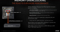 The three clock domains, according to AMD, are in a 1:1:1 synchrony, i.e. DRAM SDR clock is the same as uclk and fclk (for example, DDR4-3600 would see the memory real clock, uclk, and fclk run at 1800 MHz. AMD also appears to have increased the fclk limit to 2000 MHz with "Zen 3," so you can run memory clock at up to DDR4-4000 without having to engage the mclk:fclk 1:2 divider, which means DDR4-4000 on "Vermeer" will fetch as much of a real-world performance dividend as DDR4-3800 did for "Matisse." With AMD Ryzen, memory overclocking has been an effective way to improve overall system performance, due to the synchrony between mclk and fclk. and so, noticeable performance improvements can be had up to DDR4-4000, beyond which, you can still engage the divider to push mclk further up.
Sources:
VideoCardz, WCCFTech, Tecnopat
The first domain is fclk or Infinity Fabric clock. Each of the two CCDs (8-core CPU dies) has just one CCX (CPU core complex) with 8 cores, and hence the CCD's internal Infinity Fabric cedes relevance to the IFOP (Infinity Fabric over Package) interconnect that binds the two CCDs and the cIOD (client I/O controller die) together. The next frequency is uclk, or the internal frequency of the dual-channel DDR4 memory controller contained in the cIOD. And lastly, the mclk, or memory clock is the industry-standard DRAM frequency.
Mar 30th, 2025 03:26 EDT
change timezone
Latest GPU Drivers
New Forum Posts
- Can you guess Which game it is? (19)
- Did Nvidia purposely gimp the performance of 50xx series cards with drivers (126)
- RTX 5090 very slow while rendering or video/photo editing. (8)
- What are you playing? (23313)
- Windows 10 Vs 11, Which one too choose? (124)
- 13500 or 14500 or 12700 or 12700k (0)
- GPU Crashing System From Hibernation (10)
- Upgrade from a AMD AM3+ to AM4 or AM5 chipset MB running W10? (61)
- PCI 4.0 16x slot reported as a PCI 5.0 8x with the AMD 9070 XT Reaper GPU (39)
- The TPU UK Clubhouse (26006)
Popular Reviews
- Sapphire Radeon RX 9070 XT Pulse Review
- ASRock Phantom Gaming B850 Riptide Wi-Fi Review - Amazing Price/Performance
- Samsung 9100 Pro 2 TB Review - The Best Gen 5 SSD
- Palit GeForce RTX 5070 GamingPro OC Review
- Assassin's Creed Shadows Performance Benchmark Review - 30 GPUs Compared
- Sapphire Radeon RX 9070 XT Nitro+ Review - Beating NVIDIA
- ASRock Radeon RX 9070 XT Taichi OC Review - Excellent Cooling
- Enermax REVOLUTION D.F. 12 850 W Review
- AMD Ryzen 7 9800X3D Review - The Best Gaming Processor
- AMD Ryzen 9 9950X3D Review - Great for Gaming and Productivity
Controversial News Posts
- AMD RDNA 4 and Radeon RX 9070 Series Unveiled: $549 & $599 (260)
- MSI Doesn't Plan Radeon RX 9000 Series GPUs, Skips AMD RDNA 4 Generation Entirely (142)
- Microsoft Introduces Copilot for Gaming (124)
- AMD Radeon RX 9070 XT Reportedly Outperforms RTX 5080 Through Undervolting (119)
- NVIDIA Reportedly Prepares GeForce RTX 5060 and RTX 5060 Ti Unveil Tomorrow (115)
- Over 200,000 Sold Radeon RX 9070 and RX 9070 XT GPUs? AMD Says No Number was Given (100)
- NVIDIA GeForce RTX 5050, RTX 5060, and RTX 5060 Ti Specifications Leak (96)
- Retailers Anticipate Increased Radeon RX 9070 Series Prices, After Initial Shipments of "MSRP" Models (90)
62 Comments on AMD Ryzen 5000 Series Features Three Synchronized Memory Clock Domains
ZEN3 may need other set of settings.
We cant really know anything about it.
Who can tell, and be 100% sure, that ZEN3 can tolerate the same amount of voltages on the memory subsystem?
Dont be eager to try... a few weeks (hopefully) wont kill you. But you could kill your brand new CPU...
www.crucial.com/memory/ddr4/ct2k16g4dfra32a
I think the only confusion I remember on this is that Mark Papermaster dodged the question somewhat when interviewed by Anandtech and mentioned incremental advancements in the I/O die. He was referring to the switch from GloFo 14nm to 12nm which dropped idle power use slightly,.
from changelog:
DRAM PCB Revision - select PCB RAM for more accurate calculation of timings. In most cases it is recommended to use "A0" for better compatibility.
Anandtech and THG both officially confirmed by AMD from different sources.
In case you're wondering where any of the confusion comes from regarding the I/O die manufacturing process, all Zen2 CPUs use an I/O die fabbed on GloFo 12nm. The X570 chipset is fabbed on GloFo 14nm. You might be asking yourself what the X570 has to do with anything?
Well, they're the same thing; The X570 chipset is just a Mattise I/O die made on an older, cheaper process node. and that's why even though a Zen2 I/O die as part of a CPU uses around 12W, the X570 chipset's older 14nm process means it can draw up to 20W and necessitates active cooling.
Not a whole lot of proof out there, but I have no problem running four sticks at higher clocks and lower latencies than they're rated at.
This is the only test I've seen and it looks like the Ryzen 3000's memory controller likes four sticks of RAM and it seems to be the same across games and applications.
I guess more RAM might also help to a degree in these tests. This is also quite old and more recent AGESA/UEFI releases should have further improved things.
www.tomshardware.com/reviews/amd-ryzen-3000-best-memory-timings,6310-2.htmlWith a bit of luck, you can get some 3733MHz modules and run them at 4000MHz, at least if it works anything like my 3600MHz that I run at 3800MHz and tighter latencies.
Again, keep in mind that most memory is designed and tested for Intel or Intel and AMD's memory controller doesn't behave in the same way.
They're supposed to be 3600MHz 17-19-19-39, but they run fine at 3800MHz 16-19-16-36.
I think you'll find that 4 x dual rank sticks with any 8Gb die (B-die, CJR, Rev.E) totaling 64GB total might be a rather different, difficult and underwhelming experience.
Looks like AMD's Achilles heel (IF) won't be changing too much this generation. The UMC remains as strong if not stronger tham Matisse (already had a comparable or better memory controller than Intel), but the +200MHz is probably coming from more optimized IF traces on the substrate and the CCX layout reshuffle moving uncore components physically closer to the I/O die.
There seem to be a few people here are considering four dual rank modules, not sure if anyone ever ended up going for it though.
Supposedly later Ryzen 3000 CPUs can do 3866MHz IF already. Not a huge improvement, but an improvement nonetheless and I guess if AMD is bold enough to say 4000MHz will work, then maybe we'll see some chips doing a bit better than that.
Here are some quick tests 1:1 up to 4533 and async up to 5200 -> www.overclockers.com/forums/showthread.php/797596-G-Skill-Trident-Z-Neo-2x8GB-DDR4-3600-CL14-F4-3600C14D-16GTZNB-w-Ryzen-4650G