Thursday, December 11th 2025
Chinese SMIC Achieves 5 nm Production on N+3 Node Without EUV Tools
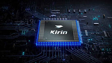
Chinese company SMIC has officially achieved volume production of its newest 5 nm-class node called SMIC N+3. This is officially China's most advanced semiconductor node produced without any extreme ultraviolet (EUV) lithography tools, relying on the deep ultraviolet (DUV) to manufacture its silicon. In the latest analysis of the Huawei Kirin 9030 SoC, the TechInsights has confirmed that the chip has officially been manufactured using the new advanced node, bringing Chinese semiconductor independence one step closer to reality. This node is a full generation ahead of the older SMIC N+2, which is 7 nm-class node Huawei has been using to manufacture its Ascend series of AI accelerators and other infrastructure parts.
However, this is not without drawbacks. Since SMIC uses DUV to print silicon designs, the company faces significant challenges in realizing its silicon ambitions. For printing smaller nodes, EUV scanners offer more possibilities due to their much smaller wavelength of 13.5 nm, compared to the smallest DUV immersion scanner wavelength of 193 nm. TechInsights has confirmed that SMIC's N+3 node, despite achieving impressive DUV multi-patterning implementation, encounters significant yield challenges, particularly due to the aggressively scaled metal pitch. As a result, the Huawei Kirin 9030 SoC is likely produced at an operating loss, with a significant portion of dies being discarded or used for downgraded chips.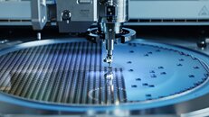
 In a single-patterning round, the best DUV immersion scanners can achieve resolutions for nodes with sub-38 nm prints. SMIC has likely optimized these machines to reach closer to 35 nm in a single print, using multiple rounds of printing to fully etch the design. Techniques like self-aligned quadruple patterning (SAQP) have been used in semiconductor nodes for years, so it is logical that SMIC has employed a similar technique with its new N+3 node. It is important to note that the majority of these DUV tools has been studied for decades, and new techniques are just refinements of what has been internally applied at test runs. TechInsights expects that the yield issues are still present, but information is limited about SMIC's node success.
In September, SMIC was testing an immersion DUV lithography scanner developed by Shanghai Yuliangsheng Technology. This move is part of an effort to establish a local wafer fabrication equipment industry and lessen reliance on Western suppliers. The Yuliangsheng system was described as an immersion DUV scanner intended for 28 nm class processes, comparable to older Twinscan designs from around 2008. However, it isn't possible that SMIC has achieved a breakthrough in such a short period, and the new DUV scanner might be domestically producing Huawei's Kirin 9030 SoC. Hence, this new SMIC N+3 node is likely made using ASML's tools.
Source:
TechInsights
However, this is not without drawbacks. Since SMIC uses DUV to print silicon designs, the company faces significant challenges in realizing its silicon ambitions. For printing smaller nodes, EUV scanners offer more possibilities due to their much smaller wavelength of 13.5 nm, compared to the smallest DUV immersion scanner wavelength of 193 nm. TechInsights has confirmed that SMIC's N+3 node, despite achieving impressive DUV multi-patterning implementation, encounters significant yield challenges, particularly due to the aggressively scaled metal pitch. As a result, the Huawei Kirin 9030 SoC is likely produced at an operating loss, with a significant portion of dies being discarded or used for downgraded chips.


In September, SMIC was testing an immersion DUV lithography scanner developed by Shanghai Yuliangsheng Technology. This move is part of an effort to establish a local wafer fabrication equipment industry and lessen reliance on Western suppliers. The Yuliangsheng system was described as an immersion DUV scanner intended for 28 nm class processes, comparable to older Twinscan designs from around 2008. However, it isn't possible that SMIC has achieved a breakthrough in such a short period, and the new DUV scanner might be domestically producing Huawei's Kirin 9030 SoC. Hence, this new SMIC N+3 node is likely made using ASML's tools.
18 Comments on Chinese SMIC Achieves 5 nm Production on N+3 Node Without EUV Tools
If I gave you a hammer and sent you off into the woods.. how long till you can send me an email?
事倍功半。
flashlight.nitecore.com/Know/detail/ad/1875
flashlight.nitecore.com/Know/detail/ad/2022
flashlight.nitecore.com/Know/detail/ad/2108
www.firefly-outdoor.com/collections/emitter-and-battery
Skilhunt also has their own homegrown LED(HighCRI in 5k Tint) but they dont have dedicated page about that LED.
Really impressive stuff they are doing even without access to the latest and greatest. It also goes to show how far behind and how slow other companies (that have advanced equipment) are. Ingenuity drives advancements. Kudus to the brilliant minds in those companies without the luxury of the best equipment.
If someone can explain to me what the point is of having a way overpriced 5nm chip relative to a way overpriced 7nm chip, I'm all ears.
This is a prestige project and a loss venture. At best, it is mildly useful in military applications where cost is no object. On a marketplace though, its not just dead, its an exercise in self destruction. You simply cannot mass produce this and get away with it for too long.Dream on :D
A more expensive chip is a one-time cost, but its power draw is recurrent and thus a more efficient chip can make up for its initial price in the medium term, specially when we're talking about larger scales and how electricity is a limited and expensive commodity.
Now, as far as I'm aware, it's possible to reach process-metrics as small as down to 1.4 Ångström (1.4nm) or so through DUVL only (using multi-patterning, obviously).
As Wizard pointed out though from a soverignty/security argument that throws the commercial argument completely on its head.