Taiwan Adds Huawei and SMIC to Export Control List, TSMC First to Comply
On June 10, Taiwan's Ministry of Economic Affairs expanded its list of strategic export-controlled customers to include Huawei and Semiconductor Manufacturing International Corporation (SMIC). The ministry announced that this decision followed a review meeting focused on preventing the proliferation of arms and other national security concerns. Moving forward, any Taiwanese exporter must obtain formal government approval before shipping semiconductors, lithography machines, or related equipment to Huawei or SMIC. TSMC immediately confirmed its full compliance. Company representatives reminded stakeholders that no orders have been fulfilled for Huawei since September 2020 and pledged to enhance internal verification procedures to block any unauthorized transactions. These steps build on one‑billion‑dollar penalty, imposed after investigators determined that two million advanced AI chiplets had been supplied for Huawei's Ascend 910B accelerator without proper clearance.
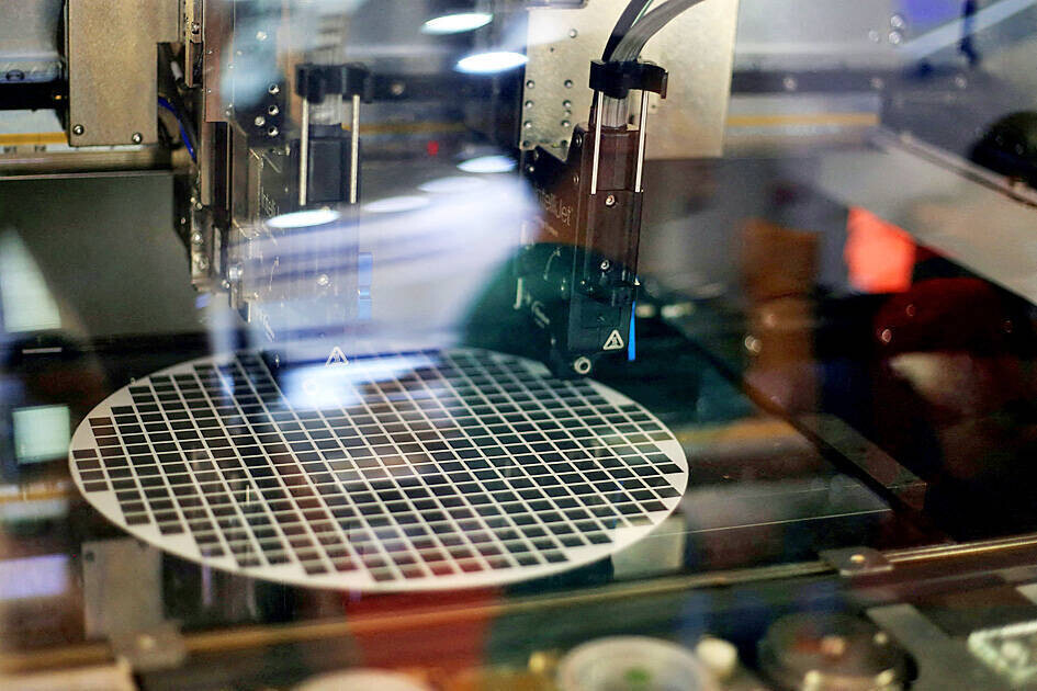
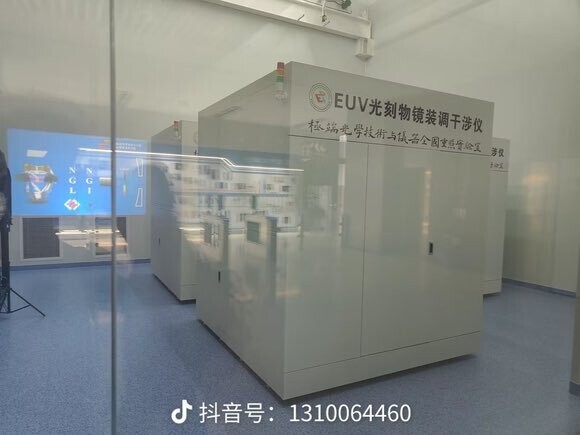
For Huawei and SMIC, this latest measure compounds the challenges created by existing US export controls, which prohibit both companies from sourcing many US-origin technologies and designs. The two Chinese giants will accelerate efforts to develop domestic alternatives, yet true semiconductor independence remains a distant goal. Designing and building reliable extreme ultraviolet lithography systems demands years of specialized research and highly precise manufacturing capabilities. Scaling production without foreign expertise could introduce costly delays. In response, Chinese research institutes report that the country's first homegrown EUV lithography machines are slated to enter trial production in the third quarter of 2025. Meanwhile, state‑backed partners are racing to develop advanced packaging tools to rival those offered by ASML. Despite these initiatives, experts warn that catching up with global leaders will require substantial time and continued investment.
For Huawei and SMIC, this latest measure compounds the challenges created by existing US export controls, which prohibit both companies from sourcing many US-origin technologies and designs. The two Chinese giants will accelerate efforts to develop domestic alternatives, yet true semiconductor independence remains a distant goal. Designing and building reliable extreme ultraviolet lithography systems demands years of specialized research and highly precise manufacturing capabilities. Scaling production without foreign expertise could introduce costly delays. In response, Chinese research institutes report that the country's first homegrown EUV lithography machines are slated to enter trial production in the third quarter of 2025. Meanwhile, state‑backed partners are racing to develop advanced packaging tools to rival those offered by ASML. Despite these initiatives, experts warn that catching up with global leaders will require substantial time and continued investment.