Saturday, December 29th 2007

NVIDIA GeForce 8800GS 192-bit 384MB and 768MB First Look
NVIDIA is going to release yet another revision to its GeForce 8 family, the GeForce 8800GS 192-bit 384MB and 768MB. A quick look at the chart below will tell you the differences between the 192-bit 8800GS and other 8 series. The price tag of 8800GS 384MB will be 1199CNY or about 164USD, while the 768MB version will cost 1499CNY (~204USD). Redirect here for some more pics and results.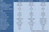

Source:
XtremeSystems Forums


56 Comments on NVIDIA GeForce 8800GS 192-bit 384MB and 768MB First Look
and saving even a few pence makes sense to the oem box makers..
trog
And please get your facts right:
5% higher mem freq does nothing for GS as 192bit bus eats away a quarter of it's memory bandwidth compared to GT.
GT:
256bit @ 900MHz (DDR1800)
= 57.6GB/s
GS:
192bit @ 950MHz (DDR1900)
= 45.6GB/s (-26.3%)
On top of that we got the 25% lower ROP count for GS - which devastates pixel fillrate:
GT:
16ROPs @ 600MHz
= 9.6GPixels/s
GS:
12ROPs @ 650MHz
= 7.8GPixels/s (-23.1%)
IMO, 768MB version can be real hottie...
One thing that brings me down - ATI. Damn, they really have to do SOMETHING. We do not want nVidia to be 'the one and only'... :/
Where's this going to stop? So many variants definitely are diluting the brand value of the 8800 series. I think NVidia is just trying to make a quick buck before the GeForce 9 series and so...we have this. Consumers are bamboozled with so much variations, they just look at the price ant make a pick. A smart ploy actually to attract people to buying a $200 Geforce 8800
Guess we won't be knowing where it places until we see actual benchmarks.
Edit: Largon's post makes sense - I wish I was capable of making those calculations myself...
The difference in ROP and memory bandwidth strength will be nothing compared to the extra 50Mhz on the 112 SPs.
The GS should be minimally inferior and a much better buy with 768MB.
But ofcourse, I could be wrong...It's really very simple, just multiply the operating frequency by amount of buswidth/shaders/TMUs/ROPs or whatever you're calculating.
Here's an example how to convert buswidth and frequency to bandwidth (GB/s):
256bit @ 900MHz (DDR1800)
= 256bit × 1800MHz
= 460800Mbit/s
Divide this by 8 and to get MB/s (8bits = 1byte):
= 57600MB/s
= 57.6GB/s
Nvidia - 7800GS (G70 256MB), 7800GT (G70 256MB),7800GTX (G70 256MB), 7800GTX 512 (G70 512MB), 7900GS (G71 256MB), 7900GT (G71 256MB) , 7900GTO (G71 512MB), 7900GTX (G71 512MB), 7900GX2 (G71 1024MB), 7950GT (G71 256MB), 7950GT (G71 512MB), 7950GX2 (G71 1024MB).
Ati - X1800 GTO (R520 256MB), X1800 GTO Rev. 2 (R520 256MB), X1800 XL (R520 256MB), AIW X1800 XL (R520 256MB), X1800 XT (R520 256MB), X1800 XT (R520 512MB), X1900 GT (R580 256MB), X1900 GT Rev. 2 (R580 256MB), AIW X1900 (R580 256MB), X1900 Crossfire Edition (R580 512MB), X1900 XT (R580 256MB), X1900 XT (R580 512MB), X1900 XTX (R580 512MB), X1950 XT (R580 256MB), X1950 XT (R580 512MB), X1950 XTX (R580+ 512MB), X1900 GT (RV570 256MB), X1900 GT (RV570 512MB), X1900 Pro (RV570 256MB), X1900 Pro (RV570 512MB).
As you can see, they have a long way to cach up to the previous generation. They should have named G92 with something like 8900 or 8850, there's no doubt about that, but this is something that has been discussed a lot too.
This doesn't mean they are going to have less GT's or GTS's, because, as I said, they have found a way to make them faster, i.e:
Before - They are able to make 100 G92 chips/hour. 40 of them are GTS, 50 GT and 10 are "failing" chips. Some of those failing could qualify as GS chips, but they are really scarce so they can't justify the creation of a new card. They probably store them somewhere.
After optimization - They are able to make 200 chips/hour. 55 are GTS, 75 are GT. Out of the remaining 70 most of them qualify as what the GS is and now there are enough of them to justify a new card in the line.
These numbers are false and exagerated, but I think they represent very well how it works. ;)