Report an Error

AMD Radeon HD 6970M X2
- Graphics Processor
- Blackcomb x2
- Cores
- 960 x2
- TMUs
- 48 x2
- ROPs
- 32 x2
- Memory Size
- 2 GB x2
- Memory Type
- GDDR5
- Bus Width
- 256 bit x2
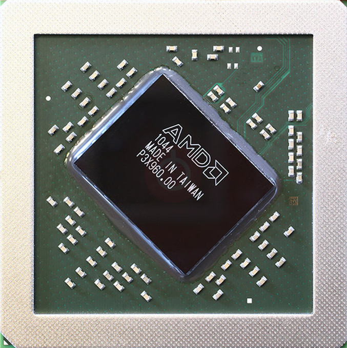
GPU
Recommended Gaming Resolutions:
- 1600x900
- 1920x1080
- 2560x1440
The Radeon HD 6970M X2 was a mobile graphics chip by AMD, launched on January 4th, 2011. Built on the 40 nm process, and based on the Blackcomb graphics processor, in its Blackcomb XT variant, the chip supports DirectX 11.2. The Blackcomb graphics processor is an average sized chip with a die area of 212 mm² and 1,700 million transistors. Unlike the fully unlocked Radeon HD 6990M, which uses the same GPU but has all 1120 shaders enabled, AMD has disabled some shading units on the Radeon HD 6970M X2 to reach the product's target shader count. Radeon HD 6970M X2 combines two graphics processors to increase performance. It features 960 shading units, 48 texture mapping units, and 32 ROPs, per GPU. AMD has paired 4 GB GDDR5 memory with the Radeon HD 6970M X2, which are connected using a 256-bit memory interface per GPU (each GPU manages 2,048 MB). The GPU is operating at a frequency of 680 MHz, memory is running at 900 MHz (3.6 Gbps effective).
Being a mxm module card, the AMD Radeon HD 6970M X2 does not require any additional power connector, its power draw is rated at 150 W maximum. This device has no display connectivity, as it is not designed to have monitors connected to it. Rather it is intended for use in laptop/notebooks and will use the output of the host mobile device.
Being a mxm module card, the AMD Radeon HD 6970M X2 does not require any additional power connector, its power draw is rated at 150 W maximum. This device has no display connectivity, as it is not designed to have monitors connected to it. Rather it is intended for use in laptop/notebooks and will use the output of the host mobile device.
Graphics Processor
- GPU Name
- Blackcomb
- GPU Variant
-
Blackcomb XT
(216-0811000)
- Architecture
- TeraScale 2
- Foundry
- TSMC
- Process Size
- 40 nm
- Transistors
- 1,700 million
- Density
- 8.0M / mm²
- Die Size
- 212 mm²
- Chip Package
- HFCBGA-1737
Mobile Graphics
Relative Performance
Based on TPU review data: "Performance Summary" at 1920x1080, 4K for 2080 Ti and faster.
Performance estimated based on architecture, shader count and clocks.
Clock Speeds
- GPU Clock
- 680 MHz
- Memory Clock
-
900 MHz
3.6 Gbps effective
Memory
- Memory Size
- 2 GB
- Memory Type
- GDDR5
- Memory Bus
- 256 bit
- Bandwidth
- 115.2 GB/s
Render Config
- Shading Units
- 960
- TMUs
- 48
- ROPs
- 32
- Compute Units
- 12
- L1 Cache
- 8 KB (per CU)
- L2 Cache
- 512 KB
Theoretical Performance
- Pixel Rate
- 21.76 GPixel/s
- Texture Rate
- 32.64 GTexel/s
- FP32 (float)
- 1,306 GFLOPS
Board Design
- Slot Width
- MXM Module
- TDP
- 150 W
- Outputs
- Portable Device Dependent
- Power Connectors
- None
- Board Number
- C296
Graphics Features
- DirectX
- 11.2 (11_0)
- OpenGL
- 4.4
- OpenCL
- 1.2
- Vulkan
- N/A
- Shader Model
- 5.0
Blackcomb GPU Notes
| Generation: Northern Islands Desktop Variant: Barts Graphics/Compute: GFX4 Display Core Engine: 5.0 Unified Video Decoder: 3.1 |
Devices based on this design (1)
| Name | GPU Clock | Memory Clock | Other Changes |
|---|---|---|---|
| 680 MHz | 900 MHz |

Jun 30th, 2024 02:27 EDT
change timezone
Latest GPU Drivers
New Forum Posts
- What prompts bios to just stop reading a NVME? (11)
- Silent install switches (3)
- Sexy Hardware Close-Up Pic Clubhouse. (10246)
- XFX RX6700(non-xt)missing one smd-capacitor for vram (27)
- Can anyone figure out what's wrong with my laptop? (11)
- ASUS VG279QR GLOW. (7)
- Anyone born in the 70s? Remember how good the 90s games were? (116)
- TPU's Nostalgic Hardware Club (18673)
- 2 vs 4 ram sticks (39)
- Monitor randomly goes black / blinks for a second then comes back (8)
Popular Reviews
- Endgame Gear OP1 8K Review
- Corsair MP600 Mini 2 TB Review - Great Storage for Steam Deck
- Bykski CPU-FIRE-ON-I CPU Water Block Review
- Lian Li HydroShift LCD 360S AIO Review
- XPG Invader X Review
- Upcoming Hardware Launches 2024 (Updated May 2024)
- XFX Radeon RX 7900 XTX Magnetic Air Review
- Sapphire Radeon RX 7600 XT Pulse Review
- AMD Ryzen 7 7800X3D Review - The Best Gaming CPU
- Patriot Viper Xtreme 5 DDR5-7600 32 GB CL36 Review
Controversial News Posts
- AMD Outs Ryzen 5000XT Processors for Socket AM4, an 8-year Old Socket (208)
- Legendary Overclocker KINGPIN Leaves EVGA and Joins PNY to Develop Next-Generation GPUs for Extreme OC (195)
- AMD Says Ryzen 9000 Series Won't Beat 7000X3D Series at Gaming (140)
- Possible Specs of NVIDIA GeForce "Blackwell" GPU Lineup Leaked (139)
- First Reviews are Live and Snapdragon X Elite Doesn't Quite Deliver on Promised Performance (124)
- ASUS Enhances Customer Support Following Gamers Nexus Investigation (118)
- Nightmare Fuel for Intel: Arm CEO Predicts Arm will Take Over 50% Windows PC Market-share by 2029 (112)
- AMD Zen 5 Storms into Gaming Desktops with Ryzen 9000 "Granite Ridge" Processors (100)