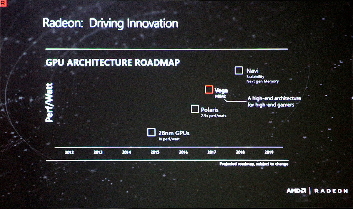
AMD Details ZEN Microarchitecture IPC Gains
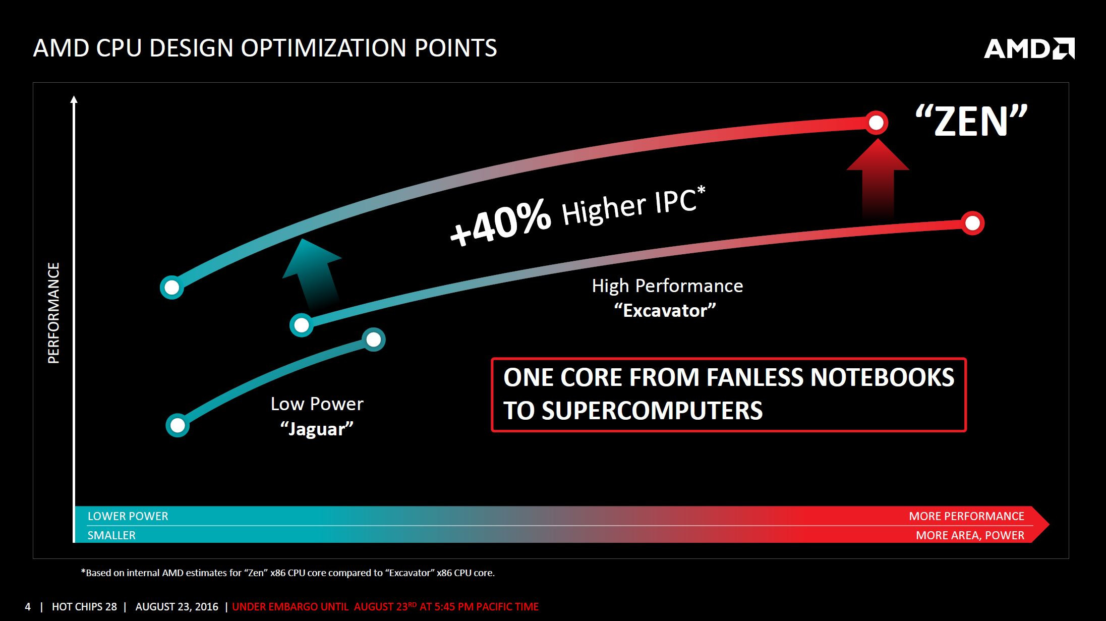
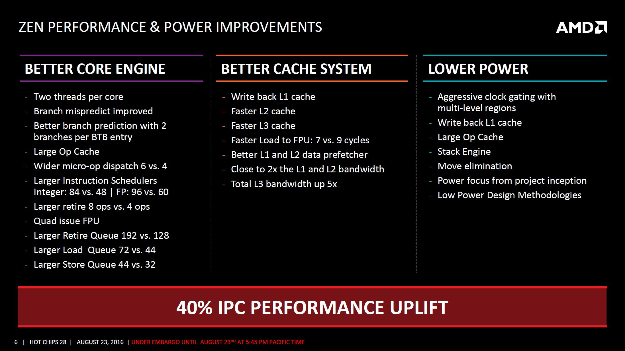
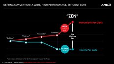
AMD Tuesday hosted a ZEN microarchitecture deep-dive presentation in the backdrop of Hot Chips, outlining its road to a massive 40 percent gain in IPC (translated roughly as per-core performance gains), over the current "Excavator" microarchitecture. The company credits the gains to three major changes with ZEN: better core engine, better cache system, and lower power. With ZEN, AMD pulled back from its "Bulldozer" approach to cores, in which two cores share certain number-crunching components to form "modules," and back to a self-sufficient core design.
Beyond cores, the next-level subunit of the ZEN architecture is the CPU-Complex (CCX), in which four cores share an 8 MB L3 cache. This isn't different from current Intel architectures, the cores share nothing beyond L3 cache, making them truly independent. What makes ZEN a better core, besides its independence from other cores, and additional integer pipelines; subtle upscaling in key ancillaries such as micro-Op dispatch, instruction schedulers; retire, load, and store queues; and a larger quad-issue FPU.
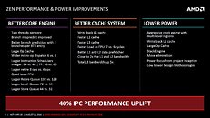
Beyond cores, the next-level subunit of the ZEN architecture is the CPU-Complex (CCX), in which four cores share an 8 MB L3 cache. This isn't different from current Intel architectures, the cores share nothing beyond L3 cache, making them truly independent. What makes ZEN a better core, besides its independence from other cores, and additional integer pipelines; subtle upscaling in key ancillaries such as micro-Op dispatch, instruction schedulers; retire, load, and store queues; and a larger quad-issue FPU.