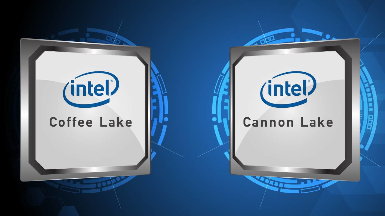
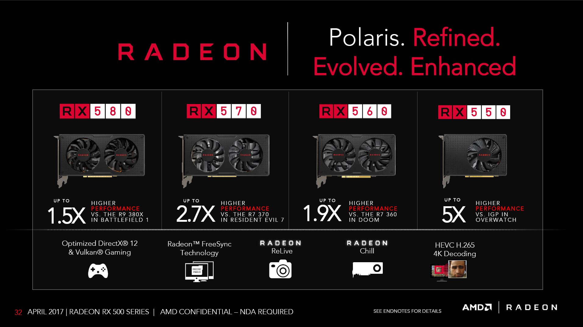
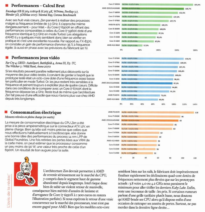
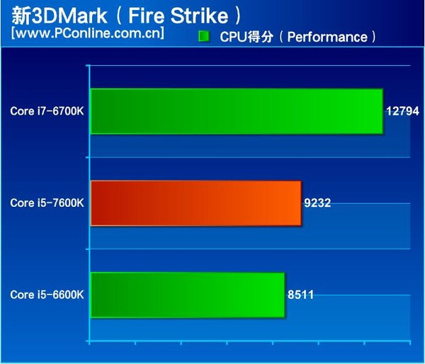
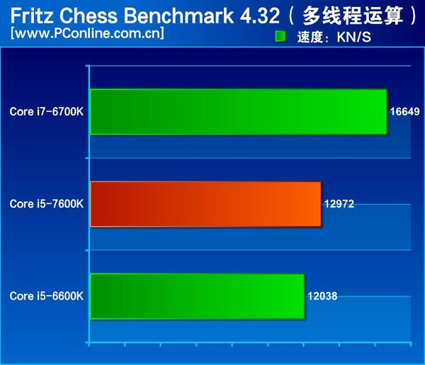
Intel to Accelerate Basin Falls Unveil, Coffee Lake Launch
According to DigiTimes, sources among Taiwan-based PC vendors have indicated that Intel's upcoming Basin Falls platform, which includes Skylake-X and Kaby Lake-X processors on a new X299 chipset, will be unveiled at Computex 2017 (May 30th, June 3rd), in Taipei - two months earlier than expected. This move comes accompanied by an accelerated launch of the Coffee Lake microarchitecture, which still uses the 14 nm process, to August 2017 from an initial January 2018 launch. If true, this is big in a number of ways - that Intel would bring forward a product launch 4 months has some interesting implications - or at least, confirmations.
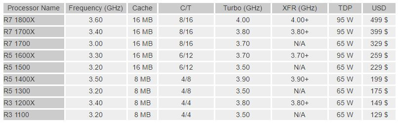
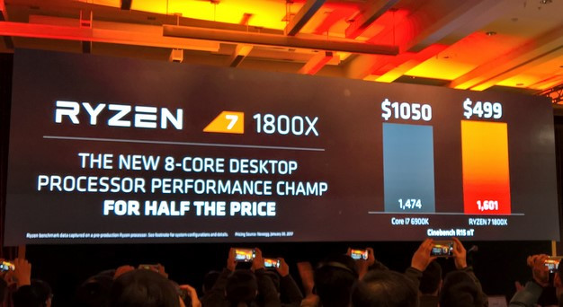
Remember that Coffee Lake is supposed to carry an increased number of cores in its mainstream designs. And we all know how Intel's line-up has almost been torn apart by Ryzen's aggressive core and thread-count, with AMD offering more cores and threads than Intel at virtually all price-points. And even if an argument is made regarding Intel's better gaming performance, that's one scenario out of many. Future proofing, professional work, multimedia, all of these assert AMD's dominance in a pure price-performance ratio. I, for one, would gladly give up some FPS in some games and accept an increased number of cores than go the other way around (especially with AMD's platform support and the number of patches that have increased game performance on Ryzen CPUs.)


Remember that Coffee Lake is supposed to carry an increased number of cores in its mainstream designs. And we all know how Intel's line-up has almost been torn apart by Ryzen's aggressive core and thread-count, with AMD offering more cores and threads than Intel at virtually all price-points. And even if an argument is made regarding Intel's better gaming performance, that's one scenario out of many. Future proofing, professional work, multimedia, all of these assert AMD's dominance in a pure price-performance ratio. I, for one, would gladly give up some FPS in some games and accept an increased number of cores than go the other way around (especially with AMD's platform support and the number of patches that have increased game performance on Ryzen CPUs.)