News Posts matching #14 nm

Return to Keyword Browsing

AMD Polaris 10 "Ellesmere" as Fast as GTX 980 Ti: Rumor

At a presser in Taiwan for its Radeon Pro Duo launch, AMD talked extensively about its upcoming "Polaris" and "Vega" family of GPUs. The company appears to be betting heavily on two SKUs it plans to launch this June, Polaris 10 and Polaris 11. Polaris 10 is an internal designation to Radeon R9 490(X), based on the 14 nm "Ellesmere" silicon. It may be the biggest chip AMD builds on the "Polaris" architecture, but it won't exactly be a "big chip," in that it doesn't succeed "Fiji." That honor is reserved for "Vega," which debuts in early-2017.

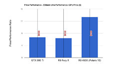
The "Ellesmere" silicon is more of AMD's competitor to NVIDIA's GP104. It is rumored that the R9 490(X), based on this silicon, will offer consumers performance rivaling the GeForce GTX 980 Ti (ergo faster than the Radeon R9 Fury X), at a USD $300-ish price point. "Ellesmere" will be a lean-machine, physically featuring up to 2,560 4th generation GCN stream processors (2,304 enabled on Polaris 10), a possible 256-bit GDDR5X memory interface, and a deep sub-200W typical board power rating.

AMD to Launch Radeon R7 470 and R9 480 at Computex

Computex 2016 could see some major consumer graphics action, with AMD reportedly planning to launch two mid-thru-performance segment products on the sidelines of the event - the Radeon R7 470, based on the 14 nm "Baffin" (Polaris 11) silicon, and the Radeon R9 480, based on the 14 nm "Ellesmere" (Polaris 10) silicon. The R7 470 could succeed the R7 370 series in not just performance, but also offer a leap in energy efficiency, with a TDP of less than 50W. The R9 480, on the other hand, could feature a TDP of just 110-135W (R9 380 is rated at 190W).

The R9 480, based on the "Ellesmere" (Polaris 10) is shaping up to be a particularly interesting silicon. It's rumored to feature 2,304 stream processors based on the 4th generation Graphics CoreNext architecture, with 2,560 stream processors being physically present on the chip; and a 256-bit wide GDDR5 (GDDR5X-ready) memory controller. 8 GB could be the standard memory amount. AMD could keep the clock speeds relatively low, with 800-1050 MHz GPU clocks. Imagine R9 390-like performance at half its power-draw.

Intel Xeon "Broadwell-EP" Launch by Month's End?

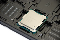
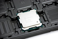
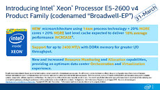
According to a leaked company slide doing rounds on the web, Intel plans to launch its workstation-grade Xeon "Broadwell-EP" processors by March 31, 2016. These chips will be branded under the Xeon E5-2600 V4 series. HP is ready with a workstation based on these chips, the HP Z640, which succeeds the Z620 that's driven by "Haswell-EP" Xeon chips. Dollar-for-Dollar, Intel is positioning the "Broadwell-EP" to offer at least "20% more cores and last-level cache" than "Haswell-EP."

This would mean Intel leveraging the 14 nm process to cram 10-core chips at the price of an 8-core chip from the previous generation, 8-core chips at the price of 6-core ones, and so on. The same slide mentions that "Broadwell-EP" offers, on average, 18% more performance than "Haswell-EP." Intel is also hinting at native support for DDR4-2400 MHz. Haswell-EP supports DDR4-2133 MHz.

AMD Unveils GPU Architecture Roadmap, "Polaris" to Skip HBM2 Memory?

Alongside its big Radeon Pro Duo flagship graphics card launch, AMD unveiled its GPU architecture roadmap that looks as far into the future as early-2018. By then, AMD will have launched as many as three new GPU architectures. It begins with the launch of its 4th generation Graphics CoreNext architecture, codenamed "Polaris," in mid-2016. Built on the 14 nm FinFET process, "Polaris" is expected to offer a whopping 2.5x increase in performance-per-Watt for AMD, compared to its current GCN 1.2 architecture on 28 nm.

Hot on Polaris' heels, in early-2017, AMD plans to launch the "Vega" GPU architecture. While this appears to offer a 50% increase in performance-per-Watt over Polaris, its highlight is HBM2 memory. Does this mean that AMD plans to skip HBM2 on Polaris, and stick to GDDR5X? Could AMD be opting for a similar approach to NVIDIA, by launching its performance-segment GPU first as an enthusiast product, giving it a free run on the markets till early-2017, and then launching a Vega-based big-chip with HBM2 memory, taking over as the enthusiast-segment product? Some time in early-2018, AMD will launch the "Navi" architecture, which appears to offer a 2.5x performance-per-Watt lead over Polaris, taking advantage of an even newer memory standard.

First 10 nm Intel Processor Out in 2017

With Intel's "tick-tock" product development cycle slowing down to a 3-launch cadence per silicon fab process, the company is preparing to launch no less than three micro-architectures on its next 10 nanometer silicon fab process. The first 10 nm CPU by Intel will launch in 2017.

In 2016, Intel will launch its 7th generation Core "Kaby Lake" processor, its third chip on the 14 nm process (after "Broadwell" and "Skylake"). The first 10 nm micro-architecture will be codenamed "Cannonlake," and will launch some time in 2017. Intel will build chips on the 10 nm for two more generations after "Cannonlake." The company's 2018 micro-architecture, built on the 10 nm will be codenamed "Icelake," and its 2019 release will be codenamed "Tigerlake." It's only 2020 that the company will pull out its next silicon fab process, 5 nm.

TSMC to Launch its 5 nm Fab by 2020

Taiwan's premier semiconductor foundry, TSMC, announced that it is on track to begin production of chips on its 7 nanometer silicon fab process by the first half of 2018. The company also announced that production on an even newer 5 nanometer process should commence two years later, in 2020. The company has currently cleared all decks for mass-production of chips on its 16 nm FFC (FinFET compact) node, with the company hoping to grab over 70% of the worldwide 14/16 nm production market-share by the end of 2016.

Intel Readies a 5.1 GHz Xeon Chip Based on the "Broadwell" Architecture

Intel's first 5-gigahertz CPU will bear an unlikely brand - Xeon. The company's upcoming Xeon E5-2602 V4 quad-core chip based on the 14 nm "Broadwell-EP" silicon, is rumored to ship with a staggering 5.10 GHz clock speed out of the box. Getting there won't be easy for this socket LGA2011v3 chip. Despite being a quad-core chip, with just four out of ten cores on the "Broadwell-EP" silicon bring physically enabled, the chip's TDP is rated at 165W. Other features include 10 MB of L3 cache, and a quad-channel DDR4 memory interface.

Samsung Announces Mass Production of 2nd Gen. 14-Nanometer FinFET Logic Process

Samsung Electronics Co., Ltd., a world leader in advanced semiconductor technology, today announced that it has begun mass production of advanced logic chips utilizing its 14 nm LPP (Low-Power Plus) process, the 2nd generation of the company's 14 nm FinFET process technology.

In leading mass production of advanced FinFET logic process, Samsung announced in Q1 of 2015 the launch of the Exynos 7 Octa processor built on the industry's first 14 nm LPE (Low-Power Early) process. With the new 14 nm LPP process, Samsung continues to demonstrate its process technology leadership, and unparalleled performance and power efficiency for its Exynos 8 Octa processor and its many foundry customers including Qualcomm Technologies, Inc. The Qualcomm Snapdragon 820 processor uses Samsung's new 14 nm LPP process and is expected to be in devices in the first half of this year.

"We are pleased to start production of our industry-leading, 2nd generation 14 nm FinFET process technology that delivers the highest level of performance and power efficiency," said Charlie Bae, Executive Vice President of Sales & Marketing, System LSI Business, Samsung Electronics. "Samsung will continue to offer derivative processes of its advanced 14 nm FinFET technology to maintain our technology leadership."

AMD Demonstrates Revolutionary 14 nm FinFET Polaris GPU Architecture

AMD provided customers with a glimpse of its upcoming 2016 Polaris GPU architecture, highlighting a wide range of significant architectural improvements including HDR monitor support, and industry-leading performance-per-watt. AMD expects shipments of Polaris architecture-based GPUs to begin in mid-2016.

AMD's Polaris architecture-based 14nm FinFET GPUs deliver a remarkable generational jump in power efficiency. Polaris-based GPUs are designed for fluid frame rates in graphics, gaming, VR and multimedia applications running on compelling small form-factor thin and light computer designs.

"Our new Polaris architecture showcases significant advances in performance, power efficiency and features," said Lisa Su, president and CEO, AMD. "2016 will be a very exciting year for Radeon fans driven by our Polaris architecture, Radeon Software Crimson Edition and a host of other innovations in the pipeline from our Radeon Technologies Group."

Samsung to Fab AMD "Zen" and "Arctic Islands" on its 14 nm FinFET Node

It has been confirmed that Samsung will be AMD's foundry partner for its next generation GPUs. It has been reported that AMD's upcoming "Arctic Islands" family of GPUs could be built on the 14 nanometer FinFET LPP (low-power Plus) process. AMD's rival NVIDIA, meanwhile, is building its next-gen "Pascal" GPU family on 16 nanometer FinFET node, likely at its traditional foundry partner TSMC.

It gets better - not only will Samsung manufacture AMD's next-gen GPUs, but also its upcoming "Zen" family of CPUs, at least a portion of it. AMD is looking to distribute manufacturing loads between two foundries, Samsung and GlobalFoundries, perhaps to ensure that foundry-level teething trouble doesn't throw its product launch cycle off the rails. One of the most talked about "Arctic Islands" GPUs is codenamed "Greenland," likely a successor to "Fiji." Sales of some of the first chips - GPUs or CPUs - made at Samsung, will begin some time in Q3 2016. Some of the other clients for Samsung's 14 nm FinFET node are Apple and Qualcomm. The company plans to speed up development of its more advanced 10 nm node to some time in 2017.

Intel 7th Generation Core "Kaby Lake" and 200-series Chipset Platform Outlined

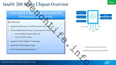
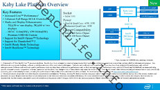
Intel's tick-tock product development cycle is disturbed. The cadence of launching a new CPU microarchitecture on a given silicon fab process, miniaturizing it to a smaller fab process, and then launching an even newer micro-architecture on that process; is about to change with the company's 7th generation Core "Kaby Lake" processor. When launched, it would be the third microarchitecture built on the company's 14 nm process, besides "Skylake" (current new architecture) and "Broadwell" (miniaturization of "Haswell" to 14 nm.) Some of the very first documents related to Kaby Lake began to move about, making news along the way. The architecture is scheduled to launch along with its companion 200-series chipset some time in 2016.

To begin with, Core "Kaby Lake" will continue to be built on the LGA1151 package, and will likely be backwards compatible with existing 100-series chipset motherboards with a firmware update. From what we get to understand from leaked material, it will not be a vastly newer architecture than Skylake, at least not of the kind Skylake was to Broadwell. There are still CPU performance enhancements on offer, an "enhanced full-range BClk overclocking," which could mean improved overclocking on chips with upwards-locked multipliers (although we won't get our hopes too high and call it a return of the BClk overclocking era). A bulk of the R&D will fall into improving the integrated graphics, to support multiple 5K displays, 10-bit HVEC and VP9 hardware-acceleration; platform-integrated Thunderbolt 3, and platform interface support for Intel Optane (3D XPoint memory).

GlobalFoundries 14 nm LPP FinFET Node Taped Out, Yields Good

GlobalFoundries' move to leapfrog several silicon fab steps to get straight to 14 nanometer (nm) is on the verge of paying off, with the company taping out its 14 nm LPP (low-power plus) FinFET node, and claiming good yields on its test/QA chips. This takes the node one step closer to accepting orders for manufacturing of extremely complex chips, such as CPUs and GPUs.

AMD is expected to remain the company's biggest client, with plans to build its next-generation "Zen" processor on this node. The company's "Arctic Islands" graphics chips are also rumored to be built on the 14 nm node, although which foundry will handle its mass production remains unclear. A big chunk of AMD's R&D budget is allocated to getting the "Zen" architecture right, with key stages of its development being handled by Jim Keller, the brains behind some of AMD's most commercially successful CPU cores.

NVIDIA "Pascal" GPUs to be Built on 16 nm TSMC FinFET Node

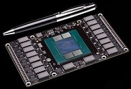
NVIDIA's next-generation GPUs, based on the company's "Pascal" architecture, will be reportedly built on the 16 nanometer FinFET node at TSMC, and not the previously reported 14 nm FinFET node at Samsung. Talks of foundry partnership between NVIDIA and Samsung didn't succeed, and the GPU maker decided to revert to TSMC. The "Pascal" family of GPUs will see NVIDIA adopt HBM2 (high-bandwidth memory 2), with stacked DRAM chips sitting alongside the GPU die, on a multi-chip module, similar to AMD's pioneering "Fiji" GPU. Rival AMD, on the other hand, could build its next-generation GCNxt GPUs on 14 nm FinFET process being refined by GlobalFoundries.

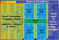
Intel "Skylake" Die Layout Detailed

At the heart of the Core i7-6700K and Core i5-6600K quad-core processors, which made their debut at Gamescom earlier this month, is Intel's swanky new "Skylake-D" silicon, built on its new 14 nanometer silicon fab process. Intel released technical documents that give us a peek into the die layout of this chip. To begin with, the Skylake silicon is tiny, compared to its 22 nm predecessor, the Haswell-D (i7-4770K, i5-4670K, etc).

What also sets this chip apart from its predecessors, going all the way back to "Lynnfield" (and perhaps even "Nehalem,") is that it's a "square" die. The CPU component, made up of four cores based on the "Skylake" micro-architecture, is split into rows of two cores each, sitting across the chip's L3 cache. This is a departure from older layouts, in which a single file of four cores lined one side of the L3 cache. The integrated GPU, Intel's Gen9 iGPU core, takes up nearly as much die area as the CPU component. The uncore component (system agent, IMC, I/O, etc.) takes up the rest of the die. The integrated Gen9 iGPU features 24 execution units (EUs), spread across three EU-subslices of 8 EUs, each. This GPU supports DirectX 12 (feature level 12_1). We'll get you finer micro-architecture details very soon.

Intel "Skylake-U" Ultra Low Power CPU Lineup Detailed

Intel's upcoming Core "Skylake-U" low-power processors, for ultra-portable notebooks, tablets, convertibles, and fan-less desktops, is where the fruition of Intel's 14 nm process takes shape. These dual-core chips, spanning all five brand extensions - Core i7, Core i5, Core i3, Pentium, and Celeron, offering TDP as low as 7.5W, and no more than 15W. The lineup is kept slim, with no more than 2 SKUs per extension. All three Core extensions feature Intel HD 520 graphics, clocked around 350 MHz, with 1000 to 1050 MHz boost, while the Pentium and Celeron models feature slimmer HD 510 graphics, ticking at 300/900 MHz.

The lineup is led by the Core i7-6600U and i7-6500U. Besides HyperThreading enabling 4 logical CPUs, these two chips feature 4 MB L3 cache, 1050 MHz iGPU boost frequency, and the highest CPU clock-speeds in the series. The Core i5 chips differ from their Core i7 counterparts with sub-3 GHz CPU clock speeds, 3 MB L3 cache, and maximum iGPU boost frequency of 1000 MHz. The Core i3 parts are almost identical to their Core i5 counterparts, except they lack CPU Turbo Boost. The Pentium processors feature very low CPU core speeds, and are almost identical to Core i3, but feature lower 950 MHz iGPU boost frequency, and 2 MB L3 cache. Celeron parts lack HyperThreading. Some of these parts will launch in 2015, others in 2016. Find the exact clock speeds for each SKU in the table below.

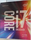
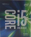
Intel Core "Skylake" Retail Boxes Surprisingly Colorful

The retail packaging of Intel's 6th generation Core "Skylake" processors in the LGA1151 package, will be surprisingly colorful, and a throwback to the pre-Pentium 4 era, according to spy-shots of the retail boxes of the upcoming Core i7-6700K and Core i5-6600K. What's even more surprising, is that packages of the i7-6700K and i5-6600K, which feature unlocked base-clock multipliers, making them primed for overclocking, do not include stock cooling solutions. Their retail packages resemble those of Intel's Core i7 HEDT processors. In the box, you'll find just the processor, its case-badge, and basic documentation.

Both the Core i7-6700K and Core i5-6600K feature the same integrated graphics SKU - HD Graphics 530. Both feature integrated memory controllers that support both DDR3L and DDR4 memory types. The Core i5 predictably lacks HyperThreading, and only features 6 MB of L3 cache, while the Core i7 features HyperThreading, and the full 8 MB present on the chip. The "Skylake" silicon will be built on the 14 nm process.

Moore's Law Buckles as Intel's Tick-Tock Cycle Slows Down

Intel co-founder Gordon Moore's claim that transistor counts in microprocessors can be doubled with 2 years, by means of miniaturizing silicon lithography is beginning to buckle. In its latest earnings release, CEO Brian Krzanich said that the company's recent product cycles marked a slowing down of its "tick-tock" product development from 2 years to close to 2.5 years. With the company approaching sub-10 nm scales, it's bound to stay that way.

To keep Moore's Law alive, Intel adopted a product development strategy it calls tick-tock. Think of it as a metronome that give rhythm to the company. Each "tock" marks the arrival of a new micro-architecture, and each "tick" marks its miniaturization to a smaller silicon fab process. Normally, each year is bound to see one of the two in alternation.

Intel's Post-2017 "Purley" Enterprise Platform Detailed

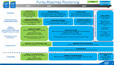
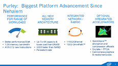
Intel's future enterprise computing business, post-2017, could see a unification of its 2-socket (2S), 4-socket (4S), and >8-socket (8S+) platforms unify into one, codenamed "Purley." The platform will consist of multiple SKUs, but a common socket type (Socket-P), and a new interconnect technology replacing InfiniBand, which will wire the sockets and core-logic across multiple server blades, together. Called Omni-Path Interconnect, the tech appears to be fiber-optic at the physical layer, with extremely thin cables, and bandwidths could start at 100 Gbps, for the first generation. The controller driving it will be codenamed "Storm Lake." The inter-socket communication will be care of a newer 10.4 GT/s UPI interconnect, each socket will feature three such UPI channels. The platform will support up to eight sockets per blade, with more sockets across neighboring blades over Omni-Path.

"Purley" will feature a new platform core-logic, in the form of the "Lewisburg" PCH. It will feature the new DMI3 chipset-bus, which is PCI-Express 3.0 x4 at the physical layer. This chipset will support up to four 10 GbE interfaces. On the processor front, will be as processors based on the "Skylake" micro-architecture. Intel will carve out several silicons based on "Skylake," the biggest one will feature 28 physical CPU cores, with HyperThreading enabling 56 logical CPUs, and for the first time, a six-channel (384-bit wide) DDR4 integrated memory controller, with support for DDR4-2666. On the flip side, this IMC only supports one DIMM per channel (DPC). The 3DPC support from previous platforms is gone. These chips will be built on the 14 nm silicon fab process, and their TDP will range between 45W and 165W, depending on the number of cores and clock speeds.

Intel Core i7-5775C and i5-5675C Hit Retail Channel in Early June

Intel's upcoming 5th generation Core processors targeted at PC enthusiasts, the Core i7-5775K, and the Core i5-5675K, will be available in the retail channel on June 1st (NA, EMEA), and June 2nd (APAC). The two were available to the OEM channel since earlier this month. This is when you will be able to buy the two at a ground store, or online, in retail (box) packaging. Built in the LGA1150 package, the two will be compatible with existing Intel 9-series chipset motherboards (with BIOS updates).

Based on the swanky new 14 nm "Broadwell" silicon, the i7-5775C and the i5-5675C are quad-core chips. The i7-5775C offers clock speeds of 3.30 GHz, which spools up to 3.70 GHz with Turbo Boost; and will feature HyperThreading, enabling 8 logical CPUs. The i5-5675C offers 3.10 GHz clocks, with 3.60 GHz Turbo Boost frequencies. Both chips will offer 6 MB of L3 cache, Intel Iris Pro 6200 graphics; and TDP as low as 65W. For this reason, and others, the two won't exactly replace the i7-4790K and i5-4690K from the product stack. The two will ship with unlocked base-clock multipliers, letting you overclock them, and could still make for great buys for premium gaming PC builds.

Intel Core i7-5775C "Broadwell" Scrapes 5 GHz OC on Air

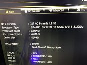
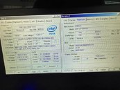
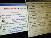
Intel's parting gifts to the LGA1150 platform, the Core i5-5675C and the Core i7-5775C, are shaping up to be a pleasant surprise to overclockers. Built on the 14 nm "Broadwell" silicon, the two quad-core chips come with extremely low rated TDP of 65W, for products of its segment. We weren't sure of those energy savings somehow translated into a massive overclocking headroom. It turns out, there's hope. Toying with a Core i7-5775C chip on an ASRock Z97 OC Formula, Hong Kong-based HKEPC found that the chip was able to reach 5.00 GHz clock speeds with ease on air-cooling, and a core voltage of 1.419V. At 4.80 GHz, the i7-5775C crunches 32M wPrime in 4.399 seconds.

ASRock Readies the Fanless BeeBox Compact Desktop

One of ASRock's prime attractions at this year's Computex, apart from its socket LGA1151 motherboards, will be a fanless compact desktop, the BeeBox. Driven by 14 nm Intel "Braswell" Celeron N3000 series SoC, the BeeBox will pack in 2 GB or 4 GB of DDR3L-1600 memory (expandable to 8 GB using two SO-DIMM slots), 32 GB to 128 GB mSATA SSD storage, and connectivity that includes 802.11 ac WLAN, gigabit Ethernet, Bluetooth 4.0, four USB 3.0 ports (including one type-C port), and display outputs that include HDMI and DisplayPort. Measuring 110 mm x 46 mm x 118.5 mm, the BeeBox will be complete quiet, including its brick-type power supply.

95W TDP of "Skylake" Chips Explained by Intel's Big Graphics Push

Intel's Core "Skylake" processor lineup, built on the company's swanky new 14 nanometer fab process, drew heads to its rather high 95W TDP for quad-core parts such as the Core i7-6700K and Core i5-6600K, even though their 22 nm predecessors, such as the i7-4770K and the i5-4670K run cooler, at 84W TDP. A new leaked slide explains the higher TDP. Apparently, Intel is going all-out with its integrated graphics implementation on Core "Skylake" chips, including onboard graphics that leverage eDRAM caches. The company is promising as much as 50% higher integrated graphics performance over "Haswell."

Although the chips have high rated TDP, the overall energy efficiency presents a different story. SoCs based on "Skylake" will draw as much as 60% lower power than "Haswell" based ones, translating into 35% longer HD video playback on portable devices running these chips. Intel's graphics performance push is driven by an almost sudden surge in display resolutions, with standards such as 4K (3840 x 2160) entering mainstream, and 5K (5120 x 2880) entering the enthusiast segment. Intel's design goal is to supply the market with a graphics solution that makes the two resolutions functional on desktop and video, if not gaming.

AMD Readies 14 nm FinFET GPUs in 2016

At its ongoing Investor Day presentation, AMD announced that will continue to make GPUs for every segment of the market. The company is planning to leverage improvements to its Graphics CoreNext architecture for the foreseeable future, but is betting on a huge performance/Watt increase with its 2016 GPUs. The secret sauce here will be the shift to 14 nm FinFET process. It's important to note here, that AMD refrained from mentioning "14 nm," but the mention of FinFET is a reliable giveaway. AMD is expecting a 2x (100%) gain in performance/Watt over its current generation of GPUs, with the shift.

AMD's future GPUs will focus on several market inflection points, such as the arrival of CPU-efficient graphics APIs such as DirectX 12 and Vulkan, Windows 10 pulling users from Windows 7, 4K Ultra HD displays getting more affordable (perhaps even mainstream), which it believes will help it sell enough GPUs to return to profitability. The company also announced an unnamed major design win, which will take shape in this quarter, and which will hit the markets in 2016.

AMD "Zen" Offers a 40% IPC Increase Over "Excavator"

In its Investor Day presentation, led by CEO Lisa Su, and CTO Mark Papermaster, AMD made a slew of careful, near-term product announcements, and market strategies. One of its announcements that strike us, is the company's emphasis on getting the CPU core design right. The company talked about its "Zen" CPU core architecture, not from a technical standpoint, on how it fits into the company's near-term. It turns out that the company is betting on a massive performance increase.

AMD announced that its "Zen" CPU core, will offer a massive 40 percent increase in IPC (instructions per clock) or in other words, performance/clock, over the existing "Excavator" CPU core architecture. Zen will introduce features such as SMT (simultaneous multi-threading), a brand new low-latency cache system, and will leverage the 14 nm FinFET process. The first products based on Zen will be desktop CPUs in the 6th generation FX processor family, which will be launched in 2016. AMD plans to unify the CPU and APU into one socket, which will be called AM4 (and not the previously thought of "FM3"). You'll be able to install both CPUs (which lack integrated graphics, but feature more CPU cores); and the company's 7th generation A-series APUs (which integrate both CPU and iGPUs), on the same kind of motherboards.
Return to Keyword Browsing
Nov 21st, 2024 10:05 EST change timezone

New Forum Posts

Popular Reviews

Controversial News Posts