News Posts matching #14 nm

Return to Keyword Browsing

Desktop OEMs Begin Listing "Broadwell" Chips, "Skylake" Arrives in Q3

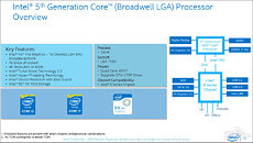
Major pre-built desktop manufacturers began listing products driven by 5th generation Core "Broadwell" processors, which are having a brief stint at the markets before being replaced by 6th generation Core "Skylake" processors in Q3-2015. The 5th Generation Core family is led by two parts, the Core i5-5675C, and the Core i7-5775C, both of which come with unlocked base-clock multipliers, are based on Intel's new 14 nanometer silicon fab process, and built in the LGA1150 package, compatible with existing Intel 9-series chipset based motherboards, with BIOS updates.

The Core i5-5675C and i7-5775C aren't exactly successors of the i5-4690K and i7-4790K. The i7-5775C is placed in a product tier Intel calls "P1+," while the i5-5675C is placed in one called "MS2+." The two aren't exactly in the same plane as P1K (eg: i7-4790K) or MS2K (eg: i5-4690K), respectively, and don't qualify as P1 (eg: i7-4790 non-K) or MS2 (eg: i5-4690 non-K). The two still feature unlocked multipliers. This places them somewhere between P1K/MS2K and P1/MS2. Both the i5-5675C and i7-5775C are quad-core chips, and physically feature just 6 MB of L3 cache. The i7-5775C has access to all 6 MB of it, while the i5-5675K features just 4 MB.

AMD Readying "Godavari" APUs for May Launch, 14 nm APUs in 2016

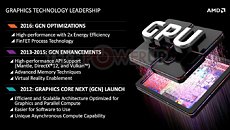
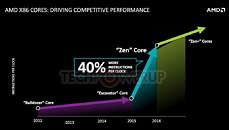
AMD is readying its next-gen APUs, codenamed "Godavari" for launch in May 2015, according to industry sources in Taiwan. A successor to "Kaveri," Godavari will feature updated "Excavator" architecture based CPU cores, and the latest Graphics CoreNext 1.2 based stream processors on the integrated GPU. The APU will feature PCI-Express gen 3.0 and high-speed DDR3 integrated memory controllers, just like its predecessor "Kaveri," and could be based on the existing FM2+ platform. These chips will compete against some of the entry/mainstream variants of Intel's Core "Broadwell" processors. It's likely that these chips could be built on existing 28 nm process.

It's also being reported that AMD will launch its first APUs based on the 14 nanometer fab process, codenamed "Summit Ridge," in 2016. These will be succeeded by "Raven Ridge" APUs in 2017. AMD could use Samsung and GlobalFoundries to make its 14 nm chips. Lastly, AMD is reportedly in talks with ASMedia to integrate its USB 3.1 controller logic into its new motherboard chipset, which it plans to launch in September 2015.

AMD to Skip 20 nm, Jump Straight to 14 nm with "Arctic Islands" GPU Family

AMD's next-generation GPU family, which it plans to launch some time in 2016, codenamed "Arctic Islands," will see the company skip the 20 nanometer silicon fab process from 28 nm, and jump straight to 14 nm FinFET. Whether the company will stick with TSMC, which is seeing crippling hurdles to implement its 20 nm node for GPU vendors; or hire a new fab, remains to be seen. Intel and Samsung are currently the only fabs with 14 nm nodes that have attained production capacity. Intel is manufacturing its Core "Broadwell" CPUs, while Samsung is manufacturing its Exynos 7 (refresh) SoCs. Intel's joint-venture with Micron Technology, IMFlash, is manufacturing NAND flash chips on 14 nm.

Named after islands in the Arctic circle, and a possible hint at the low TDP of the chips, benefiting from 14 nm, "Arctic Islands" will be led by "Greenland," a large GPU that will implement the company's most advanced stream processor design, and implement HBM2 memory, which offers 57% higher memory bandwidth at just 48% the power consumption of GDDR5. Korean memory manufacturer SK Hynix is ready with its HBM2 chip designs.

Intel to Launch Just Two LGA1150 "Broadwell" Parts

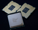
In what could be a sign of Intel being stuck with "undigested" Core "Haswell" inventories, BGA chips becoming commonplace for desktop platforms that don't see CPU upgrades, or even "Broadwell" being too short a stopgap between "Haswell" and "Skylake," the company has reportedly decided to launch just two socket LGA1150 Core "Broadwell" parts, when the silicon hits the market towards June.

Built in the 14 nm silicon fab process, "Broadwell" will bring about performance/Watt increments, and Intel doesn't appear to be in the mood to trade those in for higher clock speeds (higher performance out of the box). It's relevant to note here, that the "Broadwell" core is essentially an optical shrink of the "Haswell" CPU architecture to 14 nm, much like "Ivy Bridge" was to "Sandy Bridge," even if the silicon seating the cores itself is much different (meatier iGPU). Intel will be going in with just two parts, both of which are unlocked, for PC enthusiasts to chew on. These include the Core i7-5775C and the Core i5-5675C.

Intel Delays 14 nm "Skylake" Desktop CPU Launch

Intel reportedly delayed the launch of its next-generation "Skylake" desktop CPUs to August 2015, from its usual schedule of launching new CPUs each Q2. Skylake is Intel's next-generation CPU architecture, built on the company's new 14 nanometer silicon fab process. Sources in the motherboard industry based out of Taiwan tell DigiTimes that launch of Skylake and its companion 10-series chipset, and hence they won't be able to show their latest products at this year's Computex trade-show, in June. Intel is either tweaking production of its new chips, or is waiting for the market to digest inventories of its current-generation products.

Intel Custom Foundry Demos Industry-Leading 32 Gbps SerDes on 14 nm Process

Intel Corporation today unveiled silicon characterization results for its 1 to 32 Gbps high-speed SerDes on the 14nm process. This 32 Gbps SerDes is the second SerDes offering and adds to the previously announced 1 to 16 Gbps GP 14nm SerDes. It will be available by end of this year.

Intel's 14nm SerDes family is the second generation of SerDes offering and is built on the success of Intel's 12 and 28 Gbps SerDes, which is currently in production on Intel's 22nm Tri-gate process technology. Intel's 14nm SerDes extends the operating range while reducing power by 20 percent and area by more than 40 percent as compared to Intel's 22nm SerDes offering. This announcement marks the first time that a 32 Gbps, multiprotocol SerDes has been validated on any sub-20nm foundry process.

Intel Unveils New Dev Tools, Technologies For Tablets, Wearable Devices and PCs

Intel Corporation CEO Brian Krzanich kicked off Intel's annual technical conference with a broad set of computing initiatives and projects showing how the company is moving quickly to enable new market segments where everything is smart and connected. Krzanich and other executives announced new hardware and software developer tools, previewed upcoming Intel technologies and announced new products across several technology segments.

"With our diverse product portfolio and developer tools that span key growth segments, operating systems and form factors, Intel offers hardware and software developers new ways to grow as well as design flexibility," said Brian Krzanich, Intel CEO. "If it's smart and connected, it is best with Intel."

Intel Details Newest Microarchitecture and 14 Nanometer Manufacturing Process

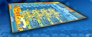
Intel today disclosed details of its newest microarchitecture that is optimized with Intel's industry-leading 14 nm manufacturing process. Together these technologies will provide high-performance and low-power capabilities to serve a broad array of computing needs and products from the infrastructure of cloud computing and the Internet of Things to personal and mobile computing.

"Intel's integrated model - the combination of our design expertise with the best manufacturing process - makes it possible to deliver better performance and lower power to our customers and to consumers," said Rani Borkar, Intel vice president and general manager of product development. "This new microarchitecture is more than a remarkable technical achievement. It is a demonstration of the importance of our outside-in design philosophy that matches our design to customer requirements."

TSMC May Lose 16 nm and 14 nm Market Share to Competitors in 2015: Chairman

TSMC may lose out on orders to competing fabs on the 16 nanometer (nm) and 14 nm nodes, in terms of market share, in 2015, according to company chairman Morris Chang. Chips built on the 16 nm node will amount to single-digit percentages of the company's output in the year. Samsung Electronics is expected to take the lead on these processes, as it just netted orders from Qualcomm, a major mobile baseband chip and SoC designer.

Chang stressed that 20 nm and 16 nm will drive revenue for the next three years for major fabs. 20 nm products will account for 10 percent of TSMC's revenues in Q3 2014, will expand to 20 percent in Q4, and contribute over 20 percent of TSMC's revenues in 2015. TSMC's 16 nm node will be competitive for products such as mobile baseband chips, ICs, GPUs, NICs, and server chips. Despite these setbacks in the company's competitive outlook, it expects its revenues to grow by 12.6 to 14.2 percent sequentially in Q3 2014, year over year.

Intel to Manufacture Panasonic System-on-Chips Using 14 nm Process

Intel Corporation today announced that it has entered into a manufacturing agreement with Panasonic Corporation's System LSI Business Division. Intel's custom foundry business will manufacture future Panasonic system-on-chips (SoCs) using Intel's 14 nm low-power manufacturing process.

Panasonic's next-generation SoCs will target audio visual-based equipment markets, and will enable higher levels of performance, power and viewing experience for consumers.

Cadence and Intel Collaborate to Enable a 14 nm Tri-gate Design Platform

Cadence Design Systems, Inc., a leader in global electronic design automation, and Intel Corporation, a world leader in computing innovation, today announced that the companies are collaborating to support Intel's 14 nm Tri-Gate process technology to enable customers of Intel Custom Foundry.

Cadence and Intel have together enabled the custom/analog flow, including Spectre APS, Virtuoso Schematic Editor, Virtuoso Layout Suite and Virtuoso Analog Design Environment for the 14nm Tri-Gate process. The companies are also collaborating on the development of the Cadence digital flow featuring Encounter Digital Implementation System, QRC Extraction Solution, and Tempus Timing Signoff Solution. Using these design flows, customers can leverage the power, performance and area benefits of Intel's 14 nm process technology.

Intel President: Integrated, Smart Connected Devices Fuel Next Era of Computing

As computing continues to evolve and expand beyond the traditional PC, Intel Corporation President Renée James said Intel and the Taiwan technology ecosystem have the exciting opportunity to build on the long history of collaborative innovation to deliver seamless and truly personal computing experiences.

Processor technology continues to get smaller with greater performance and lower power thanks to Moore's Law, expanding the scale and potential for Intel technology and that of the Taiwan ecosystem, from infrastructure for cloud computing and the Internet of Things to personal and mobile computing and wearable technology.

Samsung 14 nm FinFET Process Technology Ecosystem Solidly in Place

Stating that not all FinFETs are created equal, Samsung Electronics Co., Ltd., a global leader in advanced semiconductor solutions, today announced that the IP and design enablement ecosystem for its foundry's 14nm FinFET process technology is firmly in place as customers begin their early design work. Highlighting this fact, Samsung will be demonstrating a 14nm FinFET system-on-chip (SoC) reference board at the 51st Annual Design Automation Conference.

"To ease customers design risks moving to 14nm FinFET, we need to have all the elements of the design ecosystem optimized well in advance," said Dr. Shawn Han, vice president of foundry marketing, Samsung Electronics. "We are pleased to work with the industry's leading IP and design enablement companies. Our early work at this advanced node will allow our customers to bring their next-generation SoCs to the market quickly while taking full advantage of the benefits of our 14nm FinFET technology." Samsung's foundry offering has focused its 14nm FinFET ecosystem efforts with key IP partners. Collaboration specifically around optimal Fin-based design infrastructure and early FinFET IP development has resulted in foundation libraries and advanced IP suite. On the enablement side, Samsung, with its EDA partners, has worked to optimize 3D device modeling, extraction solutions, and design verification as well as Design for Manufacturing (DFM) solutions. The result of which is the 14nm FinFET reference board that will be on display at DAC 2014.

Intel's 14 nm "Broadwell" Could Launch by Late-2014

Intel's first processors based on the company's "Broadwell" silicon, which is an incremental upgrade to "Haswell," and built on Intel's swanky new 14 nanometer silicon fabrication process, could launch by late-2014. Intel responded to the 2014 "Back to School" shopping season with 9-series chipset motherboards featuring LGA1150 sockets, and Core "Haswell" Refresh processors. Mobile CPUs based on the silicon, were launched, too. Intel couldn't deliver on "Broadwell," the processor its 9-series chipset was originally designed to accompany. Back in 2013, "Broadwell" was expected to be Intel's big mid-2014 launch, in tune with its "Tick-Tock" product development strategy, that sees introductions of new micro-architectures, and new silicon fabrication processes take turns each year.

Samsung and GLOBALFOUNDRIES to Deliver Multi-Sourced 14 nm FinFET Offering

Samsung Electronics Co., Ltd. and GLOBALFOUNDRIES today announced a new strategic collaboration to deliver global capacity for 14 nanometer (nm) FinFET process technology. For the first time, the industry's most advanced 14 nm FinFET technology will be available at both Samsung and GLOBALFOUNDRIES, giving customers the assurance of supply that can only come from true design compatibility at multiple sources across the globe.

The new collaboration will leverage the companies' worldwide leading-edge semiconductor manufacturing capabilities, with volume production at Samsung's fabs in Hwaseong, Korea and Austin, Texas, as well as GLOBALFOUNDRIES' fab in Saratoga, New York.

Altera and Intel Extend Manufacturing Partnership

Altera Corporation and Intel Corporation today announced their collaboration on the development of multi-die devices that leverage Intel's world-class package and assembly capabilities and Altera's leading-edge programmable logic technology. The collaboration is an extension of the foundry relationship between Altera and Intel, in which Intel is manufacturing Altera's Stratix 10 FPGAs and SoCs using the 14 nm Tri-Gate process.

Altera's work with Intel will enable the development of multi-die devices that efficiently integrates monolithic 14 nm Stratix 10 FPGAs and SoCs with other advanced components, which may include DRAM, SRAM, ASICs, processors and analog components, in a single package. The integration will be enabled through the use of high-performance heterogeneous multi-die interconnect technology. Altera's heterogeneous multi-die devices provide the benefit of traditional 2.5 and 3D approaches with more favorable economic metrics. The devices will address the performance, memory bandwidth and thermal challenges impacting high-end applications in the communications, high-performance computing, broadcast and military segments.

New Intel CEO Outlines Product Plans, Future of Computing Vision at IDF 2013

From data centers to ultra-mobile devices such as tablets, phones and wearables, computing segments are undergoing exciting and even game-changing transitions, said new Intel CEO Brian Krzanich during today's opening session of the Intel Developer Forum. Krzanich laid out Intel's vision and described how Intel is addressing each dynamic market segment - such as accelerating Intel's progress in ultra-mobile devices - with new products over the next year and beyond, including a new, lower-power product family.

Krzanich said Intel plans to leave no segment untapped. "Innovation and industry transformation are happening more rapidly than ever before, which play to Intel's strengths. We have the manufacturing technology leadership and architectural tools in place to push further into lower power regimes. We plan to shape and lead in all areas of computing."
Image courtesy of Engadget

Mass Production at Intel's 14 nanometer Node Begins This Year

In addition to the industry's first fully-patterned 450 mm wafer, Intel announced that its 14 nanometer silicon fabrication node at three of its fabs will begin this year. The next leap forward from 22 nm, on which two of the company's CPU generations "Ivy Bridge" and "Haswell" are based, the 14 nm node will eventually facilitate production of the company's 5th generation Core "Broadwell" processors, which are due to arrive in 2014. Given the pace at which the 14 nm node is being developed, some of the first Broadwell Core chips, at least engineering samples, will be released to the industry within 2013. Among the three Intel facilities with 14 nm nodes are D1X, located in Oregon; Fab 42, located in Arizona; and Fab 24, located in Ireland.

Samsung Delivers Strong 14 nm FinFET Logic Process and Design Infrastructure

Samsung Electronics Co., Ltd., a global leader in advanced semiconductor solutions, today announced that it reached another milestone in the development of 14-nanometer (nm) FinFET process technology with the successful tape-out of multiple development vehicles in collaboration with its key design and IP partners. In addition, Samsung has signed an agreement with ARM for 14 nm physical IP and libraries. This agreement is the latest in a series from Samsung and ARM that has delivered production proven SoC enablement. Samsung, together with its ecosystem partners, is in a position to offer leading edge customers a robust design infrastructure to drive an ever expanding advanced mobile SoC market.

"As we move closer to true mobile computing, chip designers are eager to take advantage of the gains in performance and significantly lower power of 14 nm FinFET to deliver PC like user experience on a mobile device," said Dr. Kyu-Myung Choi, senior vice president of System LSI infrastructure design center, Device Solutions Division, Samsung Electronics. "The design complexities at 14 nm require complete harmony between the process technology, design methodology, tools and IPs. We are synchronizing all the key elements so our customers can deliver their newest chips to market quickly and efficiently."

Intel 14 nm Silicon Fab Development in Progress

Intel will be capable making chips on the 14 nanometer silicon fabrication process, in 18-inch diameter wafers, "in two years," as development of the technology and machinery to make it happen is making good progress, according to company CTO Justin Rattner. He noted that Intel's aggressive tech advancement will keep Moore's Law relevant for at least the next 10 years. By the end of 2013, Intel's D1X Fab in Oregon, Fab 42 in Arizona, in the US, and Fab 24 in Ireland will begin producing batches of simple chips such as P1272 and P1273 series SoCs. After 14 nm, development for 10 nm, 7 nm, and 5 nm will follow, in order.

Cadence Announces Tapeout of 14 nm Test-Chip

Cadence Design Systems, Inc., a leader in global electronic design innovation, announced today the tapeout of a 14-nanometer test-chip featuring an ARM Cortex-M0 processor implemented using IBM's FinFET process technology. The successful tapeout is the result of close collaboration between the three technology leaders as they teamed to build an ecosystem to address the new challenges from design through manufacturing inherent in a 14-nanometer FinFET-based design flow.

The 14-nanometer ecosystem and chip are significant milestones of a multi-year agreement between ARM, Cadence and IBM to develop systems-on-chip (SoCs) at the advanced process nodes of 14 nanometers and beyond. SoCs designed at 14 nanometers with FinFET technology offer the promise of a significant reduction in power consumption.

GLOBALFOUNDRIES Unveils FinFET Transistor Architecture for Next-Gen Mobile Devices

GLOBALFOUNDRIES today accelerated its leading-edge roadmap with the launch of a new technology designed for the expanding mobile market. The company's 14nm-XM offering will give customers the performance and power benefits of three-dimensional "FinFET" transistors with less risk and a faster time-to-market, helping the fabless ecosystem maintain its leadership in mobility while enabling a new generation of smart mobile devices.

The XM stands for "eXtreme Mobility," and it is the industry's leading non-planar architecture that is truly optimized for mobile system-on-chip (SoC) designs, providing a whole product solution from the transistor all the way up to the system level. The technology is expected to deliver a 40-60% improvement in battery life when compared to today's two-dimensional planar transistors at the 20 nm node.

NVIDIA Wants 450 mm Wafers, Seeking Foundry Partnership with GlobalFoundries, Samsung

NVIDIA is formulating a long-term chip manufacturing strategy that will see its interests secure by the time chip manufacturing has moved on to 14 nm (which follows 20 nm and today's 28 nm), which could arrive around 2015. Chip manufacturing by foundry partners is a potentially major irritant for NVIDIA, which wants to see wafer sizes getting increased from the current 300 mm manufacturing at TSMC, to 450 mm, and fast. TSMC will achieve 450 mm (18-inch) wafer manufacturing capability only by 2015. Another irritant for NVIDIA is TSMC's change in business model, which charges fabless customers "per wafer manufactured", rather than "per working chip yielded", giving them what they perceive to be the shorter end of the stick. NVIDIA is thus rigorously evaluating other foundry partners. We know from a slightly older report that Samsung has sent NVIDIA test chips manufactured at its Austin, Texas facility. There is talk that NVIDIA could also seek partnerships with GlobalFoundries, of which AMD recently relinquished all its stakes on. NVIDIA needs reliable, high-volume foundry partners that can keep it competitive not just with its main business of GPUs, but also a potential gold mine that is application processors.
Return to Keyword Browsing
Nov 21st, 2024 07:04 EST change timezone

New Forum Posts

Popular Reviews

Controversial News Posts