News Posts matching #14 nm

Return to Keyword Browsing

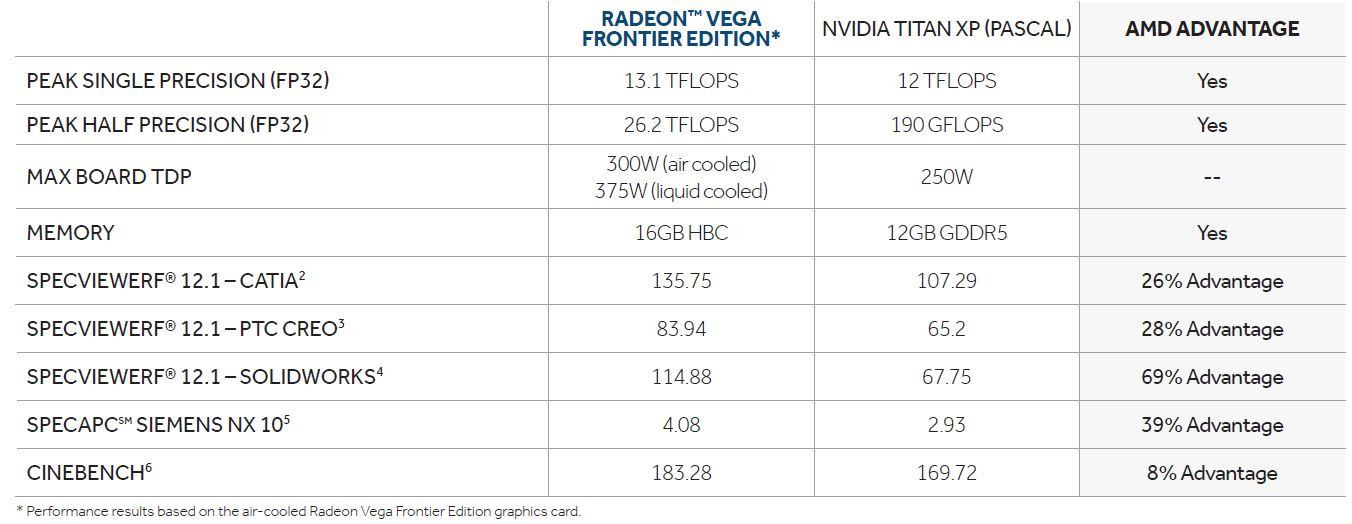
Intel Core i3-8300 Detailed - First Quad-Core i3

Intel Core i3-8300 could be the company's first quad-core processor to bear the Core i3 badge. Based on the 14 nm "Coffee Lake-S" silicon, This SKU could be priced in the upper-band of the Core i3 lineup (around the USD $150 mark), offering four cores. As if that isn't surprising enough, this quad-core chip even reportedly features HyperThreading, enabling 8 logical CPUs for the OS to deal with.

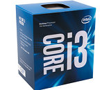
For the first time, a Core i3 part will have more logical CPUs than a Core i5 part, which lacks HyperThreading. Such a feature disparity won't be new, as current Core i3 dual-core SKUs feature HyperThreading, which Core i5 quad-core parts lack. The i3-8300, however, will lack Turbo Boost, which Core i5 SKUs will feature. The chip reportedly features a clock speed of 4.00 GHz. The L3 cache amount and TDP of this chip remain unknown at this point. Intel could launch Core i3 "Coffee Lake" processors only by late-2017 or early-2018.

AMD X399 Platform Lacks NVMe RAID Booting Support

AMD's connectivity-rich Ryzen Threadripper HEDT platform may have an Achilles's heel after all, with reports emerging that it lacks support for booting from NVMe RAID. You can still have bootable NVMe RAID volumes using NVMe RAID HBAs installed as PCI-Express add-on cards. Threadripper processors feature 64-lane PCI-Express gen 3.0 root complexes, which allow you to run at least two graphics cards at full x16 bandwidth, and drop in other bandwidth-hungry devices such as multiple PCI-Express NVMe SSDs. Unfortunately for those planning on striping multiple NVMe SSDs in RAID; the platform lacks NVMe RAID booting support. You should still be able to build soft-RAID arrays striping multiple NVMe SSDs, just not boot from them. Pro-sumers will still be able to dump their heavy data-sets onto such soft-arrays. This limitation is probably due to PCI-Express lanes emerging from different dies on the Threadripper MCM, which could present problems to the system BIOS to boot from.

Ryzen Threadripper is a multi-chip module (MCM) of two 8-core "Summit Ridge" dies. Each 14 nm "Summit Ridge" die features 32 PCI-Express lanes. On a socket AM4 machine, 4 of those 32 lanes are used as chipset-bus, leaving 28 for the rest of the machine. 16 of those head to up to two PEG (PCI-Express Graphics) ports (either one x16 or two x8 slots); and the remaining 12 lanes are spread among M.2 slots, and other onboard devices. On a Threadripper MCM, one of the two "Summit Ridge" dies has chipset-bus access; 16 lanes from each die head to PEG (a total of four PEG ports, either as two x16 or four x8 slots); while the remaining are general purpose; driving high-bandwidth devices such as USB 3.1 controllers, 10 GbE interfaces, and several M.2 and U.2 ports.

AMD Ryzen Threadripper TDP and Cache Sizes Confirmed

AMD maybe have shaken up the HEDT (high-end desktop) processor market with three Ryzen Threadripper SKU announcements early this week; but the two specifications that eluded us were their rated TDP and cache amounts. The first Ryzen Threadripper models will be available in the market from the 10th of August, and will include the 12-core/24-thread 1920X and the flagship 16-core/32-thread 1950X. Both models will feature the full 32 MB of L3 cache available from a pair of 14 nm "Summit Ridge" dies, which work out to "total cache" (L2+L3) amounts of 38 MB for the 1920X and 40 MB for the 1950X. The TDP of the 1920X and 1950X is rated at 180W. The TDP and cache configuration of the 8-core/16-thread 1900X remains unknown, for now.

It's Coffee Lake Again: Intel Six-Core Processor Surfaces on Geekbench

After rearing its head on SiSoft Sandra, it seems that an engineering sample of Intel's upcoming Coffee Lake CPUs has appeared again - this time on Geekbench. Coffee Lake is supposed to be Intel's version of a core-count democratization. It is expected that the company will introduce six-core CPUs to their i7 line of processors (since apparently the i9 moniker is now limited to the company's HEDT solutions). This should bring about a reshuffle of Intel's CPU line-up, though it remains to be seen how the company will go about that way.

Moving on to the actual Geekbench scores, Intel's 6-core, 12-thread CPU delivers a 4,619 single-core score, and a 20,828 multi-core score. This is more or less inline with AMD's Ryzen 5 1600X 6-core, 12-thread processor. However, AMD's solution is clocked higher than this particular engineering sample was (3.6 GHz on the Ryzen 5 vs 3.2 GHz on the Intel Coffee Lake sample, a 400 MHz difference.) This probably means that finalized Intel silicon with come with higher clocks, and therefore, a more commanding performance.

Intel Coffee Lake Six-core Processor Rears its Head on SiSoftware Sandra

After the absence of some further details on Intel's upcoming Coffee Lake mainstream CPU architecture (which is understandable, really, considering how the X299 platform and accompanying processors are all the rage these days), some new details have emerged. Intel's Coffee Lake architecture will still be manufactured on the company's 14 nm process, but is supposedly the last redoubt of the process, with Intel advancing to a 10 nm design with subsequent Cannon Lake.

The part in question is a six-core processor, which appears identified as a Genuine Intel CPU 0000 (so, an engineering sample.) SiSoft Sandra identifies the processor as a Kaby Lake-S part, which is probably because Coffee Lake processors aren't yet supported. The details show us a 3.1 GHz base, and a 4.2 GHz boost clock, with a 256 Kb L2 cache per core and a total of 12 MB L3 (so, 2 MB per core, which is in-line with current Kaby Lake offerings.) The 6-core "Coffee Lake" silicon will be built on a highly-refined 14 nm node by Intel, with a die-size of 149 mm². Quad-core parts won't be carved out of this silicon by disabling two cores, but rather be built on a smaller 126 mm² die.

AMD Broadens Compatibility List of DDR4 Memory for Ryzen

AMD today posted an updated compatibility list of DDR4 memory kits for Ryzen processors. While just about any DDR4 memory kit will run on socket AM4 motherboards, a limited few have been tested by AMD to run reliably at speeds such as DDR4-3200, DDR4-2933, DDR4-2667, and DDR4-2400. AMD's new compatibility list contains a wider selection of DDR4 memory modules that have been tested by AMD to work reliably on Ryzen processors.

To make the most of these modules, however, AMD asks you to look out for and install motherboard BIOS updates which contain the AGESA 1.0.0.6 micro-code update. This should be prominently displayed in the change-logs of BIOS updates from motherboard manufacturers, and the latest batches of motherboards should come with AGESA 1.0.0.6 pre-installed.
The revised DDR4 compatibility list can be accessed here.

AMD Readies B2 Stepping of the Ryzen "Summit Ridge" Silicon

AMD is readying a new stepping of its 14 nm "Summit Ridge" eight-core CPU silicon, which powers its socket AM4 Ryzen processors, according to Canard PC. The new B2 stepping reportedly addresses a lot of hardware-level errata which cannot be fixed merely by AGESA updates. According to Canard PC, the changes seem to be focused on the uncore components of "Summit Ridge." Typically, uncore refers to the integrated northbridge, which includes components such as the memory controllers, PCI-Express root complex, etc.

If the B2 stepping is mostly focused on uncore-level errata, it could mean improved PCI-Express device support, and perhaps even memory support improvements beyond even what AGESA 1.0.0.6 brings to the table. Canard PC reports that it hasn't come across any CPU core-specific errata being addressed with the B2 stepping. The glaring FMA3-related bug has been patched through BIOS updates, and most newer batches of socket AM4 motherboards come with the patch pre-installed.

AMD Radeon Pro Vega Frontier Edition TDP and Pricing Revealed

AMD Radeon Pro Vega Frontier Edition goes on sale later this month (26 June). It is designed to provide a "gateway" to the "Vega" GPU architecture for graphics professionals and game developers alike, with the consumer graphics product, the Radeon RX Vega, is bound for late-July/early-August. Radeon Pro Vega Frontier Edition, being a somewhat "enterprise-segment" product, was expected to have slightly lower TDP than its consumer-graphics sibling, since enterprise-segment implementations of popular GPUs tend to have slightly restrained clock speeds. Apparently, AMD either didn't clock the Radeon Pro Vega Frontier Edition low, or the chip has extremely high TDP.

According to specifications put out by EXXACT, a retailer which deals with enterprise hardware, the air-cooled variant of the Radeon Pro Vega Frontier Edition has a TDP rated at 300W, while its liquid-cooled variant has its TDP rated as high as 375W. To put this in perspective, the consumer-segment TITAN Xp by NVIDIA has its TDP rated at 275W. EXXACT is claiming big performance advantages in certain enterprise benchmarks such as SPECVIEWPERF and Cinebench. In other news, the air-cooled Radeon Pro Vega Frontier Edition is reportedly priced at USD $1,199; while the liquid-cooled variant is priced at $1,799. Based on the 14 nm "Vega 10" silicon, the Pro Vega Frontier Edition features 4,096 stream processors and 16 GB of HBM2 memory across a 2048-bit memory interface.

AMD Announces Radeon Pro WX 2100, WX 3100 for Workstations

AMD has recently added two new offerings to their WX series of professional, workstation-oriented graphics cards. The WX 2100 and WX 3100 are entry-level offerings for the professional market, with 512 stream processors running at 1,219 MHz on a 14 nm graphics processor based on the Polaris architecture. The RX 2100 features 2GB of GDDR5 memory on a 64-bit interface; the RX 3100 doubles those figures to 4GB of memory on a 128-bit interface.

On performance, AMD said that the soon to be released WX 2100 and WX 3100 deliver up to 2x the performance of previous entry-level professional AMD graphics, and up to 28% faster performance than competing NVIDIA offerings. The WX 2100 is expected to cost $149, while the WX 3100 is expected to go for $199. AMD said the Radeon Pro WX 2100 and WX 3100 are both expected to launch in June; an exact date wasn't provided. The company also said both cards are covered by 24/7 customer support and a three-year limited warranty that can be extended up to seven years.

Intel Announces 9th Gen Core "Cannon Lake" On Track, "Ice Lake" Taped Out

Intel announced that its first CPU micro-architecture built on its upcoming 10 nanometer silicon fab process, the 9th generation Core "Cannon Lake," is on track. In a tweet on the official company account, Intel also announced that its second micro-architecture on the new 10 nm process, codenamed "Ice Lake," is taped out.

In the wake of a competitive CPU lineup by AMD, Intel is frantically upgrading its product lineup, beginning with the new "Basin Falls" HEDT platform early-Summer 2017, followed by its 14 nm "Coffee Lake" 8th generation Core series late-Summer. "Coffee Lake" sees the first six-core SKUs to Intel's mainstream desktop lineup, which has until now, been restricted to dual-core and quad-core parts.

Intel Rushes in a Six-core Mainstream Desktop Processor by September

With AMD Ryzen 5 six-core and Ryzen 7 eight-core chips having blunt the edge of the $329 Core i7-7700K, the upper-end of Intel's mainstream desktop processor line-up has lost competitiveness to Intel's bean-counters. The company is readying a new mainstream-desktop platform, which in all likelihood, heralds a new socket, and the new Z370 Express chipset.

Intel plans to launch this platform by August-September (before Q4 sets in), and it has one big difference - a new six-core part, based on the 8th generation Core "Coffee Lake" silicon. Built on a refined 14 nm process, the 6-core "Coffee Lake" chip could feature its TDP rating around the 95W mark for the "K" (multiplier unlocked) part. Quad-core parts could also be carved out of this silicon, with their TDP rated at 65W for the non-K (multiplier-locked) parts. AMD Ryzen 7 1700 eight-core chip with unlocked multipler is rated at 65W. Intel will follow up on its first-wave of "Coffee Lake" chips with additional quad-core and dual-core parts in Q1-2018, besides other 300-series chipsets (likely the H370 and B350).

AMD Trims Prices of the Ryzen 7 1700 and 1700X

AMD recently cut the price of its current flagship desktop processor Ryzen 7 1800X from its USD $499 launch price to $469. At the time, it left prices of the Ryzen 7 1700 and Ryzen 7 1700X untouched. It looks like the two received small price-cuts as well. The Ryzen 7 1700X is now priced at $349 in leading online stores, down from its launch price of $399. The Ryzen 7 1700 (non-X), on the other hand, is now selling for $319, down from its launch price of $329. The two cuts may seem minor, but could help AMD turn up the heat against Intel's Core i7-7700K and its upcoming "Kaby Lake-X" Core i7-7740X and i5-7640X.

Based on the 14 nm "Summit Ridge" silicon, the Ryzen 7 1700 and 1700X are eight-core processors. The 1700 ships with clock speeds of 3.00 GHz, with 3.70 GHz boost, while the 1700X ships with higher 3.40 GHz clocks, with 3.80 GHz boost, and XFR, which adds a further 200 MHz to the boost clock. The Ryzen 7 1700 includes an AMD Wraith Spire RGB cooling solution, while the 1700X lacks a stock cooling solution.

Update 03/06: AMD reached out to us and commented that this is not an official price-change. It could be implemented by local retailers or distributors.

Intel Cuts Price of Core i3-7350K Overclocker-friendly Dual-core Chip

Over the weekend, Intel cut the retail price of its overclocker-friendly dual-core chip, the Core i3-7350K. The chip is now priced at USD $149, down from its launch price of $184. Based on the 14 nm "Kaby Lake" silicon, the i3-7350K is designed to target the performance-segment gaming PC crowd by offering two cores clocked extremely high out of the box, which in Intel's calculation could prove sufficient to power gaming at 1080p or even 1440p. Then there's always the joy of overclocking, thanks to its unlocked base-clock multiplier.

The Core i3-7350K features out of the box clock speeds of 4.20 GHz. Turbo Boost isn't available to the Core i3 brand. The dual-core chip features HyperThreading, enabling 4 logical CPUs for the OS to deal with. It also gets 4 MB of shared L3 cache. Its $184 launch price may have been rendered untenable by competing AMD Ryzen 5-1500X and Ryzen 5-1400 quad-core parts priced at $189 and $169, respectively, which not just give you two more cores, but also double or quadruple the L3 cache, and unlocked multipliers. Unlike the two Ryzen 5 quad-core parts, the Core i3-7350K retail package lacks a stock cooler, escalating its cost by at least another $20 for a decent cooler, if you don't have one. These factors may have driven the price-cut.

Intel "Gemini Lake" SoC Detailed

Intel is giving final touches to its next-generation "Gemini Lake" SoC, which will be sold under the Celeron and Pentium brands, and will succeed the current-generation "Apollo Lake" SoC. Built on a refined 14 nm process, the chip features a TDP of just 6W for the mobile variant, and 10W for the SFF desktop, but boasts of improved performance-per-Watt than its predecessor, translating into direct performance gains.

To begin with, "Gemini Lake" will embed a dual-core or quad-core CPU based on Intel's "Goldmont Plus" micro-architecture. A Goldmont Plus core isn't physically different from the current-gen "Goldmont," but apparently doubles the L2 cache to 4 MB from the existing 2 MB, and takes advantage of process-level improvements to lower power-draw, which Intel is using to bump up the CPU clock speeds.

AMD Ryzen 2000 Series Processors Based on Refined 14 nm Process

At its Analyst Day follow-up conference call, AMD confirmed that the company could build a new generation of Ryzen processors on 14 nm (albeit refined 14 nm) process, before transitioning to "Zen2," which will be built on the 7 nm process. As the first "Zen" based products built on the 14 nm process, the Ryzen "Summit Ridge" processors are based on the current-generation 14 nm FinFET process. AMD hopes to tap into a more refined version of this process before moving on to "Zen 2."

This could indicate that AMD's next generation of Ryzen processors, likely the Ryzen # 2xxx series, could be minor incremental updates to the current product stack, likely in the form of higher clock speeds or better energy-efficiency facilitated by the refined 14 nm process, but nothing major in the way of micro-architecture. Assuming the current Ryzen product stack, which will be augmented by Ryzen 3 series, Ryzen Pro series, and Ryzen APUs in the second half of 2017; last till mid-2018, one could expect a follow-up or refreshed Ryzen # 2xxx series run up to another year, before AMD makes a "leapfrog" upgrade to the 7 nm process with "Zen2," in all likelihood, by 2019.

Intel Pushes Motherboard + Optane Bundles, "Coffee Lake" in August

Back in April, we reported motherboard manufacturer MSI bundling Intel's Optane cache SSD with a few of its mid-range motherboards. While not free, the bundle would be slightly cheaper than the sum of its parts (buying the board and SSD separately). At the time we predicted that other motherboard vendors could launch similar bundles. It turns out that Intel is indeed coordinating motherboard + Optane SSD bundles.

In a bid to boost sales of its 200-series chipset motherboards and Core "Kaby Lake" processors, Intel is coordinating bundles of motherboards across brands with its Optane cache SSDs. Analysts predict that this could be an inventory-clearing exercise by Intel, because it plans to launch its next-generation Core "Coffee Lake" processors by late-August, 2017. "Coffee Lake" will see the introduction of six-core processor SKUs to Intel's mainstream-desktop platform, which is currently led by the quad-core i7-7700K "Kaby Lake."

AMD Intros the Radeon RX 560 Graphics Card

AMD today announced availability of the Radeon RX 560 upper-mainstream graphics card, "completing" the RX 500-series family. The company had launched the RX 500 family with the RX 550, the RX 570, and the RX 580. The RX 560 is based on the 14 nm "Polaris 11" silicon, and features 1,024 stream processors across 16 GCN compute units, 64 TMUs, 16 ROPs, and a 128-bit wide GDDR5 memory interface, holding 2 GB or 4 GB of memory. The card is clocked at 1175 MHz core, with 1275 MHz boost, and 7.00 GHz (GDDR5-effective) memory, working out to 96 GB/s of memory bandwidth. It starts at $99.

AMD Ryzen 9 Series "Threadripper" CPU Socket Detailed

AMD Ryzen 9 "Threadripper" series 12-core, 14-core, and 16-core client desktop processors, which will form the company's next-generation high-end desktop (HEDT) lineup, which goes against Intel Core i9 "Skylake-X" series, could come in a brand new socket. This shouldn't come as a surprise because the chips have higher electrical requirements, besides double the I/O of socket AM4 Ryzen processors, such as a 44-lane PCIe gen 3.0 root complex, quad-channel DDR4 memory interface, and more. This socket, according to a "HotHardware" report, is an LGA (land-grid array) with 4,094 pins.

The new LGA-4094 socket, so-called SP3r2, will be slightly scaled up from the SP3 socket AMD has been selling enterprise Opteron-brand multi-socket CPUs on (pictured below). The consumer version of this socket could feature a more user-friendly retention mechanism that shouldn't require a screwdriver to fasten. Motherboards based on this distinctively rectangular socket will feature up to eight DDR4 DIMM slots to hold quad-channel DDR4 memory, and over four PCI-Express 3.0 x16 slots, with support for 3-way and 4-way multi-GPU solutions. The motherboards will also feature copious amounts of onboard devices, M.2 slots, and other storage connectivity. Since "Threadripper" is rumored to be a multi-chip module of two 14 nm "Summit Ridge" dies linked together on-package with with an Infinity Fabric interconnect, only one of the two dies links to the motherboard chipset (AMD X399 chipset), while all the PCIe lanes of the second die (including those which would make up the chipset bus) are freed up.

BIOSTAR Intros Radeon RX 580 8GB Dual Cooling Graphics Card

BIOSTAR introduced its first custom-design Radeon RX 580 graphics card, the RX 580 8 GB Dual Cooling (model: VA5805RV82). The company had announced its foray into AMD Radeon graphics cards with a reference-design RX 580, in April. The new RX 580 Dual Cooling combines an AMD-reference design PCB with a custom-design cooling solution. This cooler features an aluminium heatsink with a copper core over the GPU; ventilated by a pair of 80 mm fans, which stay off when the GPU is idling.

The card sticks to AMD reference clock speeds of 1257 MHz core, 1340 MHz boost, and 8.00 GHz (GDDR5-effective) memory. It features 8 GB of memory over a 256-bit wide memory interface. Based on the 14 nm "Lexa" (Polaris 20) silicon, the Radeon RX 580 features 2,304 stream processors, 144 TMUs, and 32 ROPs. The card draws power from a single 8-pin PCIe power connector. Display outputs include three DisplayPort 1.4, one HDMI 2.0, and a dual-link DVI. The company didn't reveal pricing.

Intel Could Launch Core i7-7740K and "Basin Falls" Platform at E3

Intel's immediate answer to AMD's Ryzen challenge, the Core i7-7740K processor and "Basin Falls" platform, could launch on the 12th of June, 2017. Intel is the main sponsor of the PC Gaming Show hosted by PC Gamer magazine, in the backdrop of E3-2017, and we expect it to launch its first product, the Core i7-7740K on the occasion. Intel could announce retail availability of the chips immediately after. The Core i7-7740K launch will be accompanied by a more cost-effective Core i5-7640K, and the X299 Express chipset. Motherboard vendors could announce their first waves of socket LGA2066 motherboards based on this chipset.

Built on the 14 nm "Kaby Lake-X" silicon, the Core i7-7740K is a quad-core processor featuring higher clock speeds than the current i7-7700K. It features a dual-channel integrated memory controller, and lacks integrated graphics. It could feature a 28-lane PCI-Express gen 3.0 root-complex. The only ace up its sleeve is the X299 platform itself, which could be ready for bigger six-, eight-, and ten-core processors with more PCIe lane budgets.

AMD "Vega 10" Bears Core-Config Similarities to "Fiji"

A Linux patch for AMD's GPU drivers reveals that its upcoming "Vega 10" graphics processor bears numeric core-configuration similarities to the "Fiji" silicon which drives the enthusiast-segment Radeon R9 Fury series graphics cards. The patch bears configuration values which tell the software how to utilize the resources on the GPU, by spelling them out. The entry "gfx.config.max_shader_engines = 4," for example, indicates that "Vega 10" features four shader engines, like "Fiji." Another entry "Adev-> gfx.config.max_cu_per_sh = 16" signifies the number of GCN compute units (CUs) per shader engine. Assuming the number of stream processors per CU hasn't changed from 64 in the "Vega" architecture, we're looking at a total stream processor count of 4,096. This could also put the TMU count at 256.

At earlier reveals of the "Vega 10" package, you notice a large, somewhat square GPU die neighboring two smaller rectangular memory stack dies, which together sit on a shiny structure, which is the silicon interposer. The presence of just two memory stack dies sparked speculation that "Vega 10" features a narrower 2048-bit memory interface compared to the 4096-bit of "Fiji," but since the memory itself is newer-generation HBM2, which ticks at higher clocks, AMD could run them at double the memory clock as "Fiji" to arrive at the same 512 GB/s bandwidth. The 4,096 stream processors of "Vega 10" are two generations ahead of the ones on "Fiji," which together with 14 nm process-level improvements, could run at much higher GPU clocks, making AMD get back into the high-end graphics segment.

Intel Readies 34 Xeon Gold and Xeon Platinum Processor Models

Intel is preparing a new nomenclature for its Xeon line of enterprise processors based on core counts. The Xeon Bronze-3000 series will consist of chips with less than 10 cores, Xeon Silver-4000 series with 10 to 12 cores, Xeon Gold-6000 series with 14 to 22 cores, and the top-dog Xeon Platinum-8000 series with 24 to 28 cores. The company will address a variety of enterprise workstation and server markets with these chips. All chips in this lineup will be built in the new LGA-2066 package, and the Xeon Bronze and Xeon Silver parts are confirmed to be based on the "Skylake" microarchitecture.

What is also characteristic of these chips is their vast memory controller with six memory channels, and support for three DIMMs per channel. The top-tier Xeon Platinum-8000 series 28-core chip features 1 MB of dedicated L2 cache per core, and 38.5 MB of shared L3 cache. Its TDP is rated at 208W, and it will be built on Intel's 14 nm process. The 28-core parts come with clock speeds under 2.50 GHz. The 34 Xeon Gold and Xeon Platinum series processors Intel plans to launch over the year are tabled below.

AMD Ryzen 7 1800X Gets a Small Price Cut

AMD has given its flagship Ryzen processor, the Ryzen 7 1800X, a small price cut. The chip is now priced at USD $469 on leading online retailers in the US, down from its launch price of $499. This $30 cut, however, isn't spread over to AMD's other Ryzen 7 series parts. The Ryzen 7 1700X continues to go for $399, and the Ryzen 7 1700 (non-X) around $329. Prices of the Ryzen 5 series six-core and quad-core parts seem unaffected, too.

AMD's flagship processor, the Ryzen 7 1800X features eight cores, SMT enabling 16 logical CPUs for the software to deal with, 512 KB of L2 cache per core, and 16 MB of shared L3 cache. It is clocked at 3.60 GHz, with 4.00 GHz TurboCore frequency, and XFR (extended frequency range) unlocking higher automated overclocks depending on the effectiveness of your cooler. The socket AM4 chip is built on the 14 nm process, and has a 95W TDP rating.

ZOTAC Announces its ZBOX Desktops with Celeron "Apollo Lake" SoCs

ZOTAC announced a product update to its iconic ZBOX mini-PCs with new-generation Celeron "Apollo Lake" SoCs. The new ZOTAC Nano CI327 mini-PC is driven by a Celeron N3450 chip built on the 14 nm process, which embeds a quad-core "Goldmont" CPU clocked at 2.20 GHz, 2 MB of L2 cache, and Intel HD 500 graphics based on the Gen 9 LP architecture.

Measuring 127.8 mm x 126.8 mm x 56.8 mm, the ZBOX CI327 features two SO-DIMM slots that support up to 8 GB of memory, a 9 mm-thick 2.5-inch drive bay with SATA 6 Gb/s interface, a 3-in-1 card reader, a 10 Gb/s USB 3.1 type-C port, two USB 3.0 type-A ports, 802.11ac WLAN with Bluetooth 4.0, and gigabit Ethernet. Display outputs include D-Sub, HDMI 2.0 and DisplayPort 1.2. The company didn't reveal pricing.

NVIDIA Readies the GeForce GT 1030 to Compete with Radeon RX 550

With the Tuesday (18/04) launch of the Radeon RX 550 at US $79, the market for IGP-replacement discrete GPUs sprung back to life. NVIDIA is preparing to address the market with the new GeForce GT 1030 graphics card, based on its "Pascal" architecture. The SKU will be based on the new 14 nm "GP108" silicon, and could feature up to 512 CUDA cores, and up to 2 GB of GDDR5 memory across a 128-bit wide interface.

With tiny board and electrical footprints, one can expect the chip to rely on the PCI-Express slot entirely for its power, and come in low-profile and fan-less designs. It could feature an up-to-date I/O, including HDMI 2.0b and DisplayPort 1.4, which its predecessor, the GT 730 lacks. The company could formally announce the GT 1030 around mid-May, 2017.
Return to Keyword Browsing
Jun 30th, 2025 17:48 CDT change timezone

New Forum Posts

Popular Reviews

TPU on YouTube

Controversial News Posts