Tuesday, August 18th 2015

Intel "Skylake" Die Layout Detailed
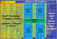
At the heart of the Core i7-6700K and Core i5-6600K quad-core processors, which made their debut at Gamescom earlier this month, is Intel's swanky new "Skylake-D" silicon, built on its new 14 nanometer silicon fab process. Intel released technical documents that give us a peek into the die layout of this chip. To begin with, the Skylake silicon is tiny, compared to its 22 nm predecessor, the Haswell-D (i7-4770K, i5-4670K, etc).
What also sets this chip apart from its predecessors, going all the way back to "Lynnfield" (and perhaps even "Nehalem,") is that it's a "square" die. The CPU component, made up of four cores based on the "Skylake" micro-architecture, is split into rows of two cores each, sitting across the chip's L3 cache. This is a departure from older layouts, in which a single file of four cores lined one side of the L3 cache. The integrated GPU, Intel's Gen9 iGPU core, takes up nearly as much die area as the CPU component. The uncore component (system agent, IMC, I/O, etc.) takes up the rest of the die. The integrated Gen9 iGPU features 24 execution units (EUs), spread across three EU-subslices of 8 EUs, each. This GPU supports DirectX 12 (feature level 12_1). We'll get you finer micro-architecture details very soon.
What also sets this chip apart from its predecessors, going all the way back to "Lynnfield" (and perhaps even "Nehalem,") is that it's a "square" die. The CPU component, made up of four cores based on the "Skylake" micro-architecture, is split into rows of two cores each, sitting across the chip's L3 cache. This is a departure from older layouts, in which a single file of four cores lined one side of the L3 cache. The integrated GPU, Intel's Gen9 iGPU core, takes up nearly as much die area as the CPU component. The uncore component (system agent, IMC, I/O, etc.) takes up the rest of the die. The integrated Gen9 iGPU features 24 execution units (EUs), spread across three EU-subslices of 8 EUs, each. This GPU supports DirectX 12 (feature level 12_1). We'll get you finer micro-architecture details very soon.

82 Comments on Intel "Skylake" Die Layout Detailed
Of course, this sucks, and it sucks even worse when you know that Intel does nothing at least to try to develop software environment to unleash all those wasted transistors.
40% of the die - to be not used.
I mean, I would know if I didn't know that Intel had provided developer guides since 2011:
software.intel.com/en-us/articles/intel-graphics-developers-guides
Or if I had missed when Intel put support behind OpenCL back in 2014:
streamcomputing.eu/blog/2014-03-25/intel-promotes-opencl-as-the-heterogeneous-compute-solution/
Or didn't attend any of the numerous Intel-sponsored development events every year:
software.intel.com/en-us/
The only thing really missing is decent graphics. This is filling that gap. No, enthusiasts don't like it, but they also make up like 10% of the market if I'm being generous...
Joke apart that's exactly the problem: the Red team is not putting up a fight and Intel can do as they please.
Problem is, considering what AMD did with Fury I'm not hoping much for their next FX series (if there is one).
Using a GPU while browsing, fapping, e.t.c. consumes much more power than having the iGPU enabled and turning on and off the dGPU for the heavy staff.
Also, your dGPU lives longer, unless you use nVidia and nVidia decides when to cripple your h/w.
The complaints won't stop until Intel gets rid of the GPU, and they really won't stop because Intel is not going to take that GPU off. This die is going to power the other desktop i5s and i7s and those are parts intended for powering a 1080P monitor at work without the assistance of a dGPU. Not throwing money into the water for a pointless GPU-less Skylake design that basically gets them no $$$ at all is actually a pretty smart business plan, believe it or not.
Not a lot of praise where it's deserved, I'm afraid. I wouldn't be showering Intel with praise 24/7, but I didn't see any positive comments about the 5820K when it was released, only "only 28 PCIe lanes? What if I need the extra 12 to get maximum performance while getting off every day?" Tried to appease the enthusiasts with a 6-core HEDT part below $400, well, I guess that didn't work out very well, did it? The 5820K wasn't even a forced hand; it could very well have been a carbon copy of the 4820K, just on Haswell, as there are 4-core E5 V3s a-plenty to prove that.
Give people something better, and they'll find something better to complain about.
you took my words...
point #2: intel knows pretty much the problem and differences about soldering and thermal paste on their CPU die's.....
but they still use that shitty paste... so?