News Posts matching #CoWoS

Return to Keyword Browsing

Major CSPs Aggressively Constructing AI Servers and Boosting Demand for AI Chips and HBM, Advanced Packaging Capacity Forecasted to Surge 30~40%

TrendForce reports that explosive growth in generative AI applications like chatbots has spurred significant expansion in AI server development in 2023. Major CSPs including Microsoft, Google, AWS, as well as Chinese enterprises like Baidu and ByteDance, have invested heavily in high-end AI servers to continuously train and optimize their AI models. This reliance on high-end AI servers necessitates the use of high-end AI chips, which in turn will not only drive up demand for HBM during 2023~2024, but is also expected to boost growth in advanced packaging capacity by 30~40% in 2024.

TrendForce highlights that to augment the computational efficiency of AI servers and enhance memory transmission bandwidth, leading AI chip makers such as Nvidia, AMD, and Intel have opted to incorporate HBM. Presently, Nvidia's A100 and H100 chips each boast up to 80 GB of HBM2e and HBM3. In its latest integrated CPU and GPU, the Grace Hopper Superchip, Nvidia expanded a single chip's HBM capacity by 20%, hitting a mark of 96 GB. AMD's MI300 also uses HBM3, with the MI300A capacity remaining at 128 GB like its predecessor, while the more advanced MI300X has ramped up to 192 GB, marking a 50% increase. Google is expected to broaden its partnership with Broadcom in late 2023 to produce the AISC AI accelerator chip TPU, which will also incorporate HBM memory, in order to extend AI infrastructure.

TSMC Showcases New Technology Developments at 2023 Technology Symposium

TSMC today showcased its latest technology developments at its 2023 North America Technology Symposium, including progress in 2 nm technology and new members of its industry-leading 3 nm technology family, offering a range of processes tuned to meet diverse customer demands. These include N3P, an enhanced 3 nm process for better power, performance and density, N3X, a process tailored for high performance computing (HPC) applications, and N3AE, enabling early start of automotive applications on the most advanced silicon technology.

With more than 1,600 customers and partners registered to attend, the North America Technology Symposium in Santa Clara, California is the first of the TSMC's Technology Symposiums around the world in the coming months. The North America symposium also features an Innovation Zone spotlighting the exciting technologies of 18 emerging start-up customers.

Chinese GPU Maker Biren Technology Loses its Co-Founder, Only Months After Revealing New GPUs

Golf Jiao, a co-founder and general manager of Biren Technology, has left the company late last month according to insider sources in China. No official statement has been issued by the executive team at Biren Tech, and Jiao has not provided any details regarding his departure from the fabless semiconductor design company. The Shanghai-based firm is a relatively new startup - it was founded in 2019 by several former NVIDIA, Qualcomm and Alibaba veterans. Biren Tech received $726.6 million in funding for its debut range of general-purpose graphics processing units (GPGPUs), also defined as high-performance computing graphics processing units (HPC GPUs).

The company revealed its ambitions to take on NVIDIA's Ampere A100 and Hopper H100 compute platforms, and last August announced two HPC GPUs in the form of the BR100 and BR104. The specifications and performance charts demonstrated impressive figures, but Biren Tech had to roll back its numbers when it was hit by U.S Government enforced sanctions in October 2022. The fabless company had contracted with TSMC to produce its Biren range, and the new set of rules resulted in shipments from the Taiwanese foundry being halted. Biren Tech cut its work force by a third soon after losing its supply chain with TSMC, and the engineering team had to reassess how the BR100 and BR104 would perform on a process node larger than the original 7 nm design. It was decided that a downgrade in transfer rates would appease the legal teams, and get newly redesigned Biren silicon back onto the assembly line.

TSMC Launches OIP 3DFabric Alliance to Shape the Future of Semiconductor and System Innovations

TSMC today announced the Open Innovation Platform (OIP) 3DFabric Alliance at the 2022 Open Innovation Platform Ecosystem Forum. The new TSMC 3DFabric Alliance is TSMC's sixth OIP Alliance and the first of its kind in the semiconductor industry that joins forces with partners to accelerate 3D IC ecosystem innovation and readiness, with a full spectrum of best-in-class solutions and services for semiconductor design, memory modules, substrate technology, testing, manufacturing, and packaging. This alliance will help customers achieve speedy implementation of silicon and system-level innovations and enable next-generation HPC and mobile applications using TSMC's 3DFabric technologies, a comprehensive family of 3D silicon stacking and advanced packaging technologies.

"3D silicon stacking and advanced packaging technologies open the door to a new era of chip-level and system-level innovation, and also require extensive ecosystem collaboration to help designers navigate the best path through the myriad options and approaches available to them," said Dr. L.C. Lu, TSMC fellow and vice president of design and technology platform. "Through the collective leadership of TSMC and our ecosystem partners, our 3DFabric Alliance offers customers an easy and flexible way to unlocking the power of 3D IC in their designs, and we can't wait to see the innovations they can create with our 3DFabric technologies."

AMD's CEO Lisa Su Planning Trip to Taiwan, Said to be Visiting TSMC to Secure Future Wafer Allocation

Based on a report by Tom's Hardware, AMD's CEO Lisa Su is planning a trip to Taiwan in the next couple of months. It is said that she is planning to meet with multiple partners in Taiwan, such as ASUS, Acer and maybe more importantly, ASMedia, which will be the sole maker of chipsets for AMD, once the X570 chipset is discontinued. AMD is apparently also seeing various less well known partners that deliver parts for its CPUs, such as Nan Ya PCB, Unimicron Technologies and Kinsus Interconnects.

However, it appears that the main reason for Lisa Su herself to visit Taiwan will be to meet with TSMC, to discuss future collaboration with CC Wei, TSMC's chief executive. This is so AMD can secure enough wafer allocation on future nodes, such as its 3 nm and 2 nm class nodes. The move to these nodes is obviously not happening in the near future for AMD, but considering that TSMC is currently the leading foundry and is operating at capacity, it makes sense to get in early, as the competition is stiff when it comes to getting wafer allocation on cutting edge nodes. It's unclear which exact 3 nm class node AMD will be aiming for, but it might be the N3P node, which is said to kick off production sometime next year. Lisa Su is also said to have meetings with TSMC, SPIL and Ase Technology when it comes to advanced packaging for AMD's products. This includes technologies such as chip-on-wafer-on-substrate (CoWoS) and fan-out embedded bridge (FO-EB), with AMD already being expected to use some of these technologies in its upcoming Navi 3x GPUs.

Biren Technology Unveils BR100 7 nm HPC GPU with 77 Billion Transistors

Chinese company Biren Technology has recently unveiled the Biren BR100 HPC GPU during their Biren Explore Summit 2022 event. The Biren BR100 features an in-house chiplet architecture with 77 billion transistors and is manufactured on a 7 nm process using TSMC's 2.5D CoWoS packaging technology. The card is equipped with 300 MB of onboard cache alongside 64 GB of HBM2E memory running at 2.3 TFLOPs. This combination delivers performance above that of the NVIDIA Ampere A100 achieving 1024 TFLOPs in 16-bit floating point operations.

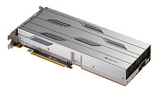
The company also announced the BR104 which features a monolithic design and should offer approximately half the performance of the BR100 at a TDP of 300 W. The Biren BR104 will be available as a standard PCIe card while the BR100 will come in the form of an OAM compatible board with a custom tower cooler. The pricing and availability information for these cards is currently unknown.

NVIDIA H100 SXM Hopper GPU Pictured Up Close

ServeTheHome, a tech media outlet focused on everything server/enterprise, posted an exclusive set of photos of NVIDIA's latest H100 "Hopper" accelerator. Being the fastest GPU NVIDIA ever created, H100 is made on TSMC's 4 nm manufacturing process and features over 80 billion transistors on an 814 mm² CoWoS package designed by TSMC. Complementing the massive die, we have 80 GB of HBM3 memory that sits close to the die. Pictured below, we have an SXM5 H100 module packed with VRM and power regulation. Given that the rated TDP for this GPU is 700 Watts, power regulation is a serious concern and NVIDIA managed to keep it in check.

On the back of the card, we see one short and one longer mezzanine connector that acts as a power delivery connector, different from the previous A100 GPU layout. This board model is labeled PG520 and is very close to the official renders that NVIDIA supplied us with on launch day.

Tianshu Zhixin Big Island GPU is a 37 TeraFLOP FP32 Computing Monster

Tianshu Zhixin, a Chinese startup company dedicated to designing advanced processors for accelerating various kinds of tasks, has officially entered the production of its latest GPGPU design. Called "Big Island" GPU, it is the company's entry into the GPU market, currently dominated by AMD, NVIDIA, and soon Intel. So what is so special about Tianshu Zhixin's Big Island GPU, making it so important? Firstly, it represents China's attempt of independence from the outside processor suppliers, ensuring maximum security at all times. Secondly, it is an interesting feat to enter a market that is controlled by big players and attempt to grab a piece of that cake. To be successful, the GPU needs to represent a great design.

And great it is, at least on paper. The specifications list that Big Island is currently being manufactured on TSMC's 7 nm node using CoWoS packaging technology, enabling the die to feature over 24 billion transistors. When it comes to performance, the company claims that the GPU is capable of crunching 37 TeraFLOPs of single-precision FP32 data. At FP16/BF16 half-precision, the chip is capable of outputting 147 TeraFLOPs. When it comes to integer performance, it can achieve 317, 147, and 295 TOPS in INT32, INT16, and IN8 respectively. There is no data on double-precision floating-point numbers, so the chip is optimized for single-precision workloads. There is also 32 GB of HBM2 memory present, and it has 1.2 TB of bandwidth. If we compare the chip to the competing offers like NVIDIA A100 or AMD MI100, the new Big Island GPU outperforms both at single-precision FP32 compute tasks, for which it is designed.
Tianshu Zhixin Big Island Tianshu Zhixin Big Island Tianshu Zhixin Big Island Tianshu Zhixin Big Island
Pictures of possible solutions follow.

Chinese Tianshu Zhixin Announces Big Island GPGPU on 7 nm, 24 billion Transistors

Chinese company Shanghai Tianshu Zhixin Semiconductor Co., Ltd., commonly known (at least in Asia) as Tianshu Zhixin, has announced the availability of their special-purpose GPGPU, affectionately referred to as Big Island (BI). The BI chip is the first fully domestic-designed solution for the market it caters to, and features close to the latest in semiconductor manufacturing, being built on a 7 nm process featuring 2.5D CoWoS (chip-on-wafer-on-substrate) packaging. The chip is built towards AI and HPC applications foremost, with applications in other industries such as education, medicine, and security. The manufacturing and packaging processes seem eerily similar to those available from Taiwanese TSMC.

Tianshu Zhixin started work on the BI chip as early as 2018, and has announced that the chip features support for most AI and HPC data processing formats, including FP32, FP16, BF16, INT32, INT16, and INT8 (this list is not exhaustive). The company says the chip offers twice the performance of existing mainstream products on the market, and emphasizes its price/performance ratio. The huge chip (it packs as many as 24 billion transistors) is being teased by the company as offering as much as 147 TFLOPs in FP126 workloads, compared to 77.97 TFLOPs in the NVIDIA A100 (54 billion transistors) and 184.6 TFLOPS from the AMD Radeon Instinct MI100 (estimated at 50 billion transistors).

TSMC to Enter Mass Production of 6th Generation CoWoS Packaging in 2023, up to 12 HBM Stacks

TSMC, the world's leading semiconductor manufacturing company, is rumored to start production of its 6th generation Chip-on-Wafer-on-Substrate (CoWoS) packaging technology. As the silicon scaling is getting ever so challenging, the manufacturers have to come up with a way to get as much performance as possible. That is where TSMC's CoWoS and other chiplet technologies come. They allow designers to integrate many integrated circuits on a single package, making for a cheaper overall product compared to if the product used one big die. So what is so special about 6th generation CoWoS technology from TSMC, you might wonder. The new generation is said to enable a massive 12 stacks of HBM memory on a package. You are reading that right. Imagine if each stack would be an HBM2E variant with 16 GB capacity that would be 192 GB of memory on the package present. Of course, that would be a very expensive chip to manufacture, however, it is just a showcase of what the technology could achieve.

Update 16:44 UTC—TheEnglish DigiTimes report indicates that this technology is expected to see mass production in 2023.

TSMC Begins Construction of 2 nm Manufacturing Facility

TSMC, the leading semiconductor foundry in the world, has reportedly begun construction of its 2 nm manufacturing facility. According to a DigiTimes report, translated by @chiakokhua on Twitter, besides the construction of 2 nm R&D center, TSMC has also started the construction of the manufacturing facility for that node, so it will be ready in time. Please do note that the node name doesn't represent the size of the transistor, so it will not actually be 2 nm wide. The new facilities will be located near TSMC's headquarters in Hsinchu Science Park, Taiwan. The report also confirms the first details about the node, specifically that it will use Gate-All-Around (GAA) technology. And there is also another interesting piece of information regarding even smaller node, the planning for 1 nm node has begun according to the source.

Besides advanced nodes, TSMC also laid out clear plans to accelerate the push of advanced packaging technology. That includes SoIC, InFO, CoWoS, and WoW. All of these technologies are classified as "3D Fabric" by the company, even though some are 2.5D. These technologies will be mass-produced at "ZhuNan" and "NanKe" facilities starting in the second half of 2021, and are expected to significantly contribute to the company's profits. It is also reported that the competing foundry, Samsung, has a 3D packaging technology of its own called X-cube, however, it is attracting customers a lot slower than TSMC due to the high costs of the new technology.

Rambus Advances HBM2E Performance to 4.0 Gbps for AI/ML Training Applications

Rambus Inc. (NASDAQ: RMBS), a premier silicon IP and chip provider making data faster and safer, today announced it has achieved a record 4 Gbps performance with the Rambus HBM2E memory interface solution consisting of a fully-integrated PHY and controller. Paired with the industry's fastest HBM2E DRAM from SK hynix operating at 3.6 Gbps, the solution can deliver 460 GB/s of bandwidth from a single HBM2E device. This performance meets the terabyte-scale bandwidth needs of accelerators targeting the most demanding AI/ML training and high-performance computing (HPC) applications.

"With this achievement by Rambus, designers of AI and HPC systems can now implement systems using the world's fastest HBM2E DRAM running at 3.6 Gbps from SK hynix," said Uksong Kang, vice president of product planning at SK hynix. "In July, we announced full-scale mass-production of HBM2E for state-of-the-art computing applications demanding the highest bandwidth available."

TSMC Details 3nm N3, 5nm N5, and 3DFabric Technology

TSMC on Monday kicked off a virtual tech symposium, where it announced its new 12 nm N12e node for IoT edge devices, announced the new 3DFabric Technology, and detailed progress on its upcoming 5 nm N5 and 3 nm N3 silicon fabrication nodes. The company maintains that the N5 (5 nm) node offers the benefits of a full node uplift over its current-gen N7 (7 nm), which recently clocked over 1 billion chips shipped. The N5 node incorporates EUV lithography more extensively than N6/N7+, and in comparison to N7 offers 30% better power at the same performance, 15% more performance at the same power, and an 80% increase in logic density. The company has commenced high-volume manufacturing on this node.

2021 will see the introduction and ramp-up of the N5P node, an enhancement of the 5 nm N5 node, offering a 10% improvement in power at the same performance, or 5% increase in performance at the same power. A nodelet of the N5 family of nodes, called N4, could see risk production in Q4 2021. The N4 node is advertised as "4 nm," although the company didn't get into its iso-power/iso-performance specifics over the N5 node. The next major node for TSMC will be the 3 nm N3 node, with massive 25%-30% improvement in power at the same performance, or 10%-15% improvement in performance at same power, compared to N5. It also offers a 70% logic density gain over N5. 3DFabric technology is a new umbrella term for TSMC's CoWoS (chip on wafer on substrate), CoW (chip on wafer), and WoW (wafer on wafer) 3-D packaging innovations, with which it plans to offer packaging innovations that compete with Intel's various new 3D chip packaging technologies on the anvil.

TSMC Sees Higher Demand for CoWoS Packaging

TSMC, Taiwan's flagship manufacturer of silicon, has seen a substantial increase in demand for Chip-on-Wafer-on-Substrate (CoWoS) packaging technology, according to the report from DigiTimes. CoWoS is a multi-chip packaging technology that gives an option to build silicon like LEGO, allowing for dies to be placed side by side on interposer that is providing high interconnect density and performance. You can see more about CoWoS in detail here. Some of the examples of CoWoS are NVIDIA's P100 and V100 dies that integrate logic (computing elements), and memory (in the form of HBM) on a single die.

Recently, TSMC updated its CoWoS technology, where this new second-generation parts could scale far larger than the first-generation implementation - up to 1700 squared millimeters of die space, allowing for some very creative solutions to be implemented. This may be the reason that the demand in Q2 has risen so substantially and that TSMC's production lines are now running at full capacity, trying to meet the demand for this packaging technology.
TSMC CoWoS NVIDIA V100
Return to Keyword Browsing
Nov 21st, 2024 12:44 EST change timezone

New Forum Posts

Popular Reviews

Controversial News Posts