Suppliers More Willing to Acquiesce on Price, 3Q22 DRAM Pricing Decline Expands to Nearly 10%, Says TrendForce
According to the latest TrendForce research, despite the rapid weakening of overall consumer demand in 1H22, DRAM manufacturers previously presented a tough stance on price negotiations and gave little ground, steadily conveying inventory pressure from buyers to sellers. Facing uncertain peak-season demand in 2H22, some DRAM suppliers have begun effectively expressing clear intentions to cut prices, especially in the server field, where demand is relatively stable, in order to reduce inventory pressure. This situation will cause 3Q22 DRAM pricing to drop from the previous 3~8% to nearly 10% QoQ. If a price war is incited due to companies competing for sales, the drop in prices may exceed 10%.
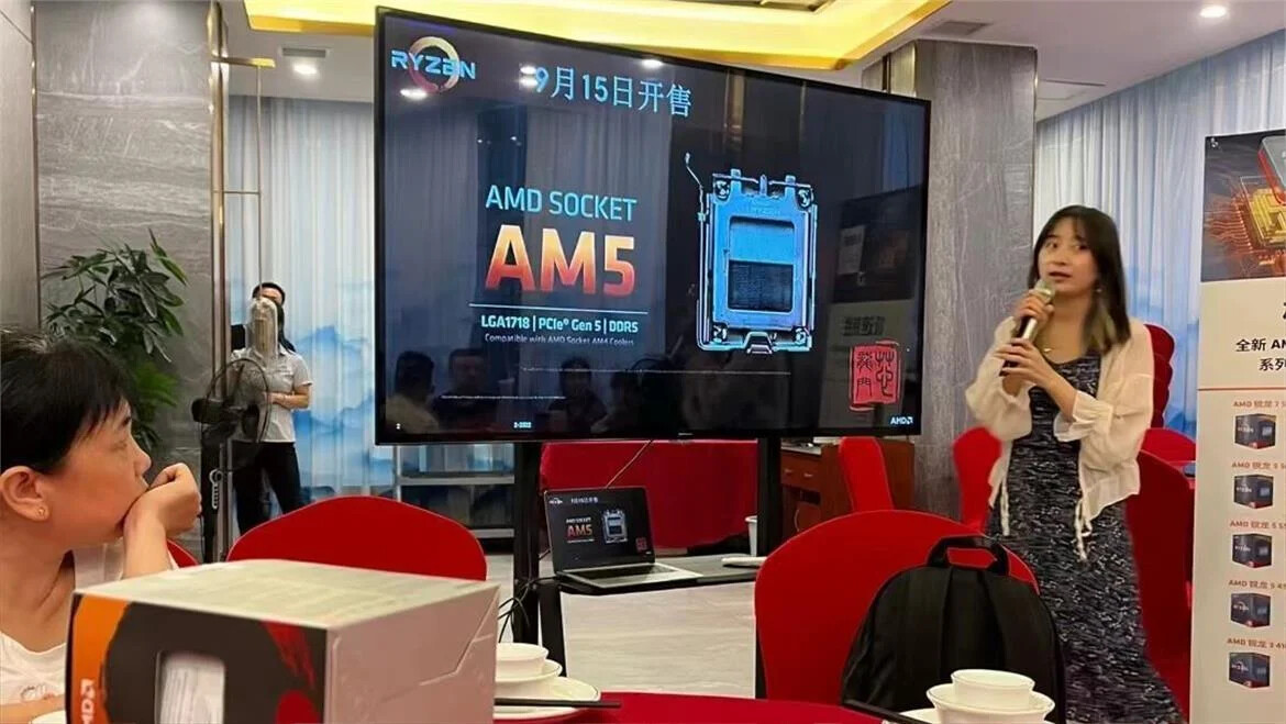
PC OEMs have continuously downgraded their shipment prospects. With average DRAM inventory levels at more than two months, unless a huge price incentive exists, there is no urgent demand for procurement. At the same time, thanks to continuous adoption of the advanced 1Z/1alpha process, supply continued to increase in 3Q22. DDR4 output could not be effectively reduced due to high pricing limiting the penetration rate of DDR5. The price decline of PC DRAM in 3Q22 is revised to 5~10%.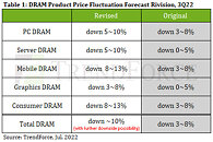
PC OEMs have continuously downgraded their shipment prospects. With average DRAM inventory levels at more than two months, unless a huge price incentive exists, there is no urgent demand for procurement. At the same time, thanks to continuous adoption of the advanced 1Z/1alpha process, supply continued to increase in 3Q22. DDR4 output could not be effectively reduced due to high pricing limiting the penetration rate of DDR5. The price decline of PC DRAM in 3Q22 is revised to 5~10%.