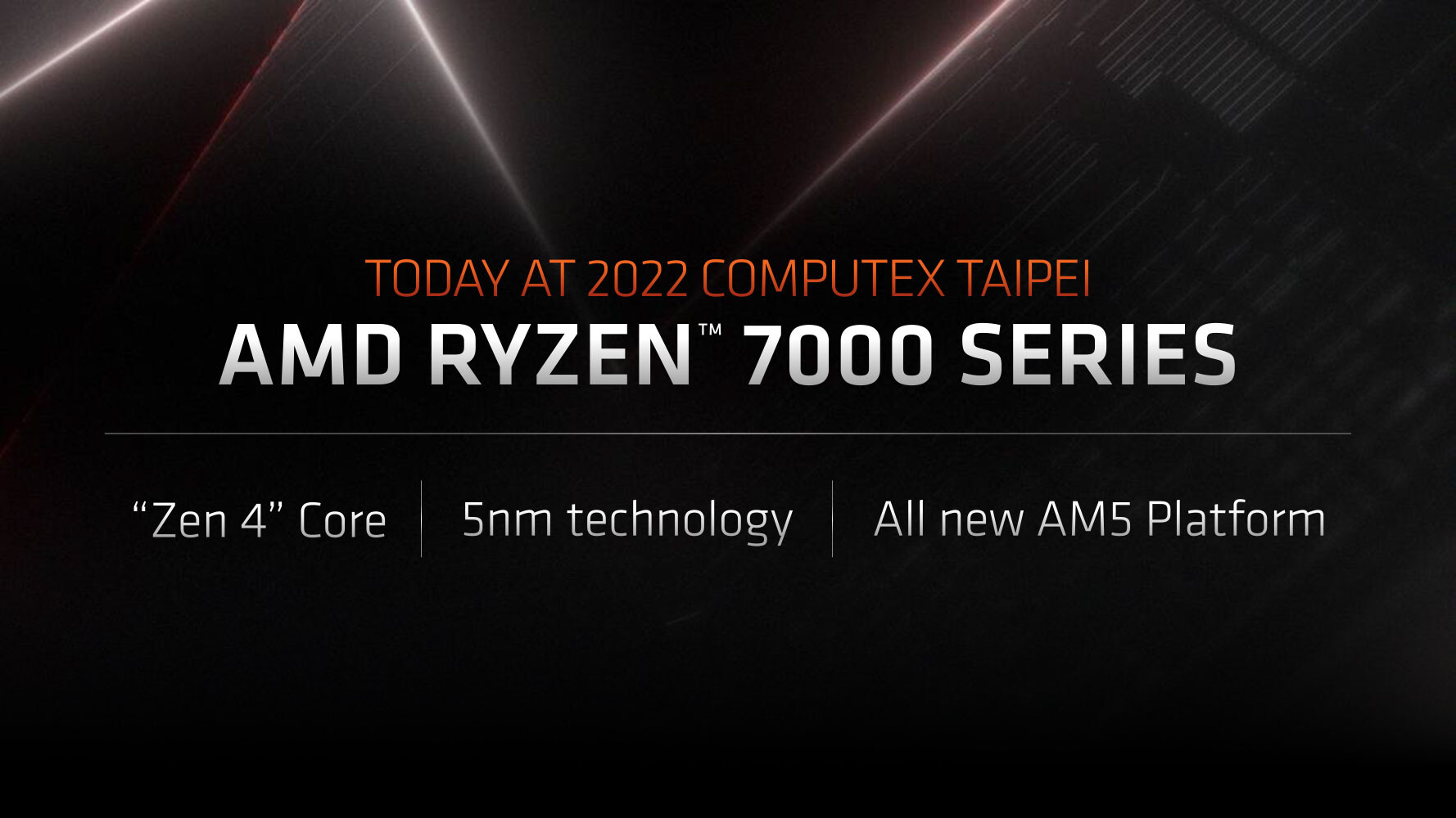
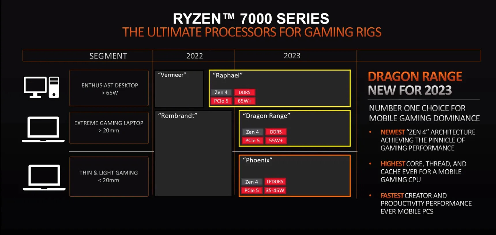
AMD Unveils 5 nm Ryzen 7000 "Zen 4" Desktop Processors & AM5 DDR5 Platform
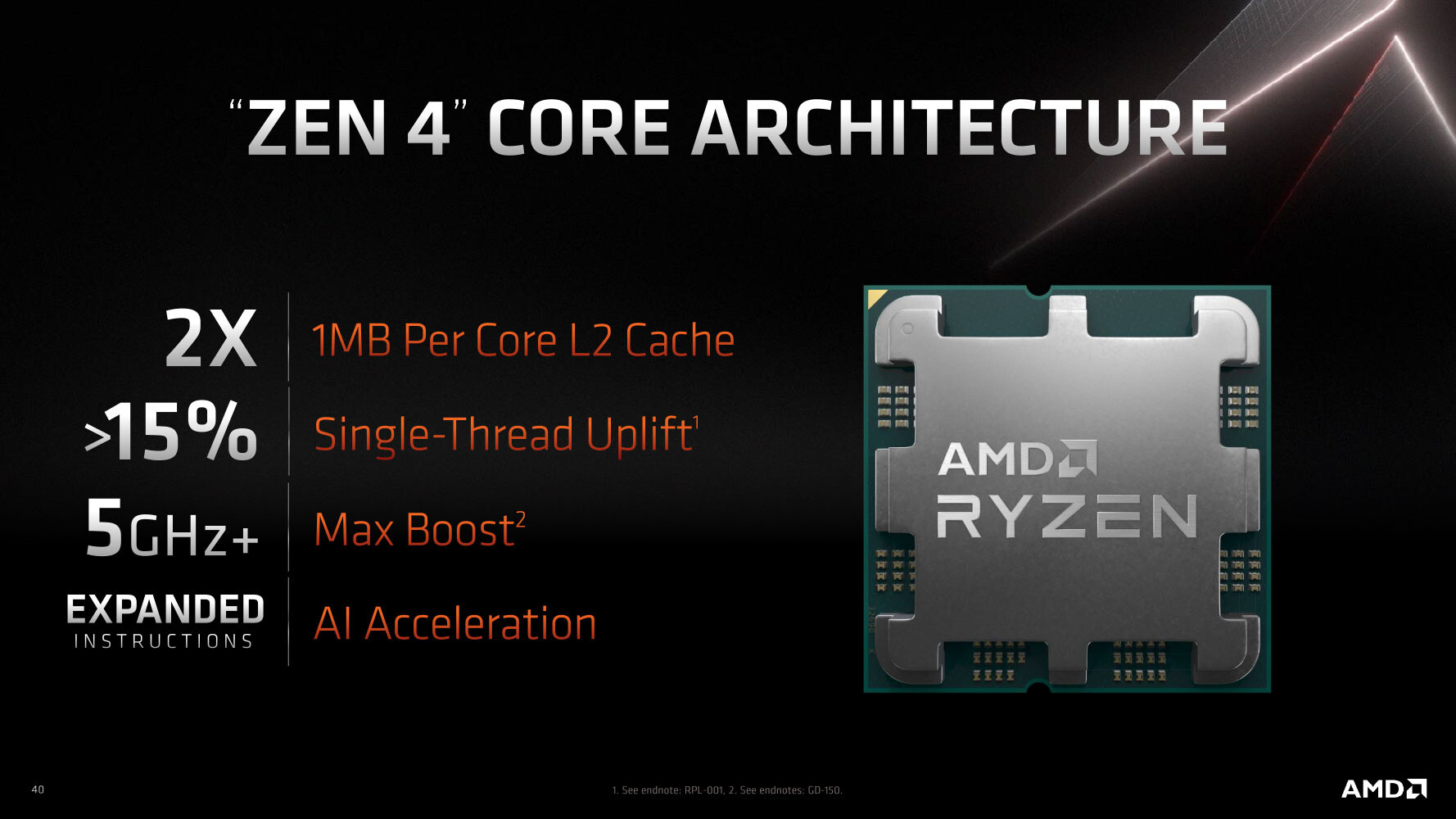
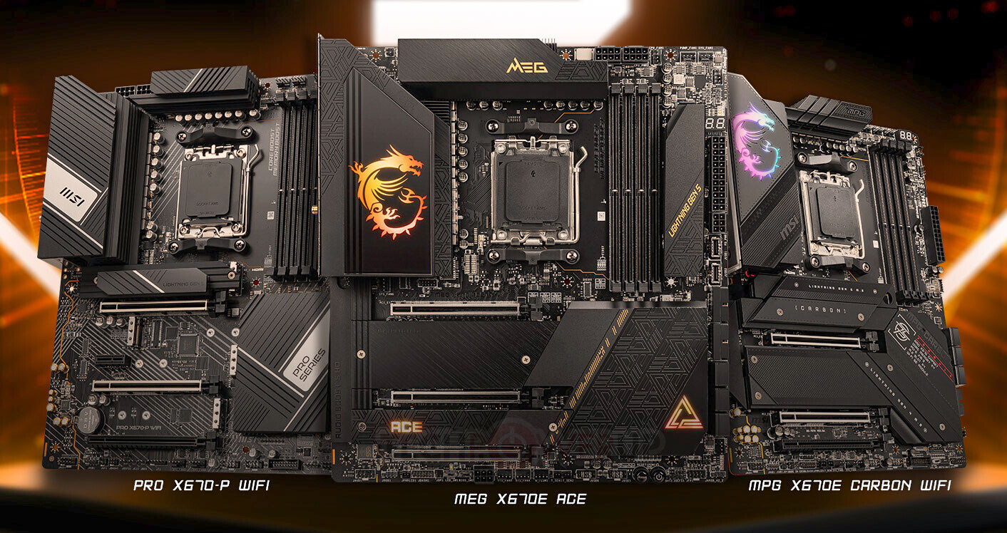
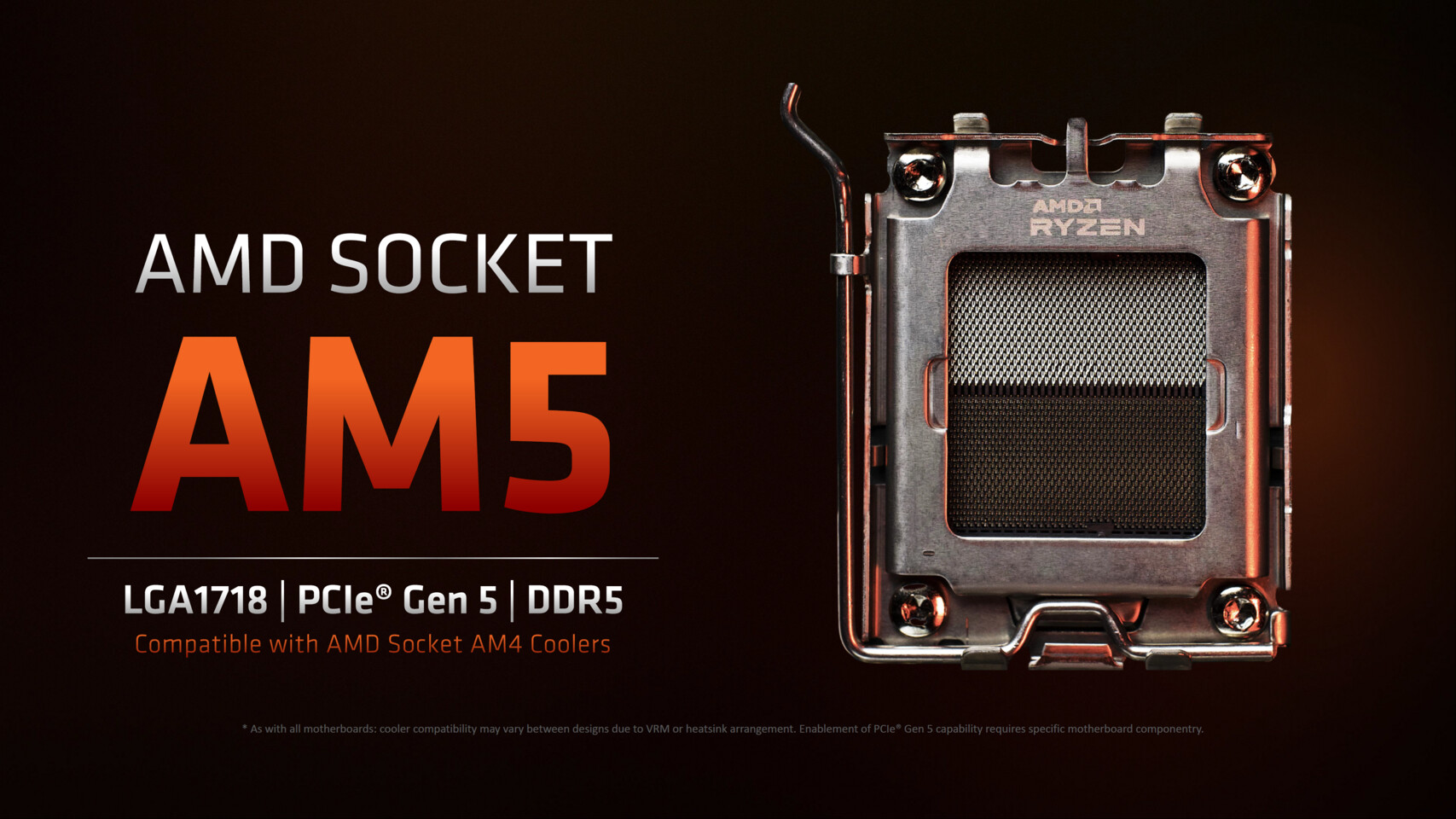
AMD today unveiled its next-generation Ryzen 7000 desktop processors, based on the Socket AM5 desktop platform. The new Ryzen 7000 series processors introduce the new "Zen 4" microarchitecture, with the company claiming a 15% single-threaded uplift over "Zen 3" (16-core/32-thread Zen 4 processor prototype compared to a Ryzen 9 5950X). Other key specs about the architecture put out by AMD include a doubling in per-core L2 cache to 1 MB, up from 512 KB on all older versions of "Zen." The Ryzen 7000 desktop CPUs will boost to frequencies above 5.5 GHz. Based on the way AMD has worded their claims, it seems that the "+15%" number includes IPC gains, plus gains from higher clocks, plus what the DDR4 to DDR5 transition achieves. With Zen 4, AMD is introducing a new instruction set for AI compute acceleration. The transition to the LGA1718 Socket AM5 allows AMD to use next-generation I/O, including DDR5 memory, and PCI-Express Gen 5, both for the graphics card, and the M.2 NVMe slot attached to the CPU socket.
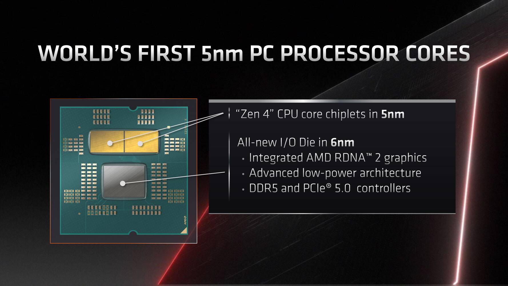
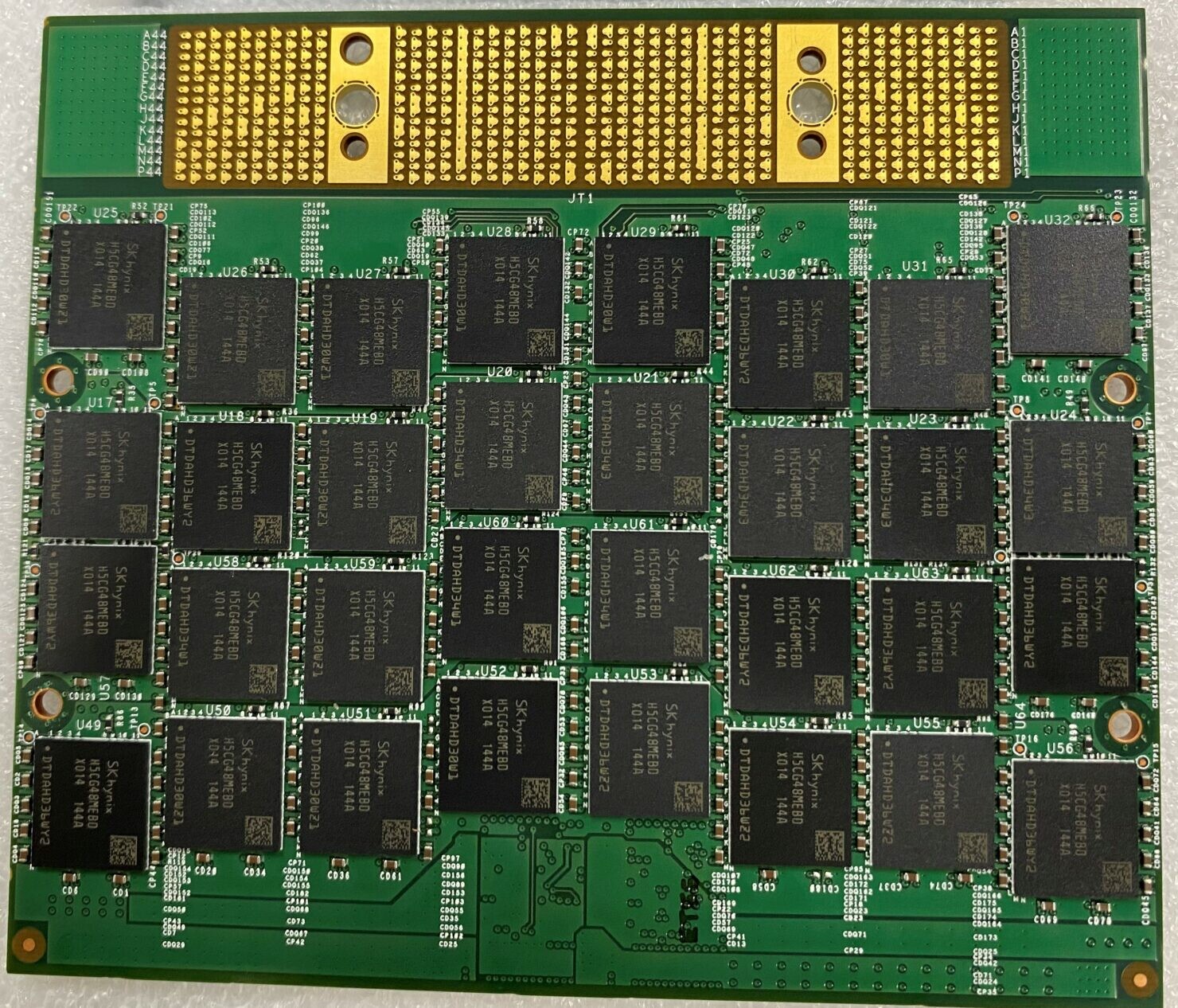
Much like Ryzen 3000 "Matisse," and Ryzen 5000 "Vermeer," the Ryzen 7000 "Raphael" desktop processor is a multi-chip module with up to two "Zen 4" CCDs (CPU core dies), and one I/O controller die. The CCDs are built on the 5 nm silicon fabrication process, while the I/O die is built on the 6 nm process, a significant upgrade from previous-generation I/O dies that were built on 12 nm. The leap to 5 nm for the CCD enables AMD to cram up to 16 "Zen 4" cores per socket, all of which are "performance" cores. The "Zen 4" CPU core is larger, on account of more number-crunching machinery to achieve the IPC increase and new instruction-sets, as well as the larger per-core L2 cache. The cIOD packs a pleasant surprise—an iGPU based on the RDNA2 graphics architecture! Now most Ryzen 7000 processors will pack integrated graphics, just like Intel Core desktop processors.


Much like Ryzen 3000 "Matisse," and Ryzen 5000 "Vermeer," the Ryzen 7000 "Raphael" desktop processor is a multi-chip module with up to two "Zen 4" CCDs (CPU core dies), and one I/O controller die. The CCDs are built on the 5 nm silicon fabrication process, while the I/O die is built on the 6 nm process, a significant upgrade from previous-generation I/O dies that were built on 12 nm. The leap to 5 nm for the CCD enables AMD to cram up to 16 "Zen 4" cores per socket, all of which are "performance" cores. The "Zen 4" CPU core is larger, on account of more number-crunching machinery to achieve the IPC increase and new instruction-sets, as well as the larger per-core L2 cache. The cIOD packs a pleasant surprise—an iGPU based on the RDNA2 graphics architecture! Now most Ryzen 7000 processors will pack integrated graphics, just like Intel Core desktop processors.