News Posts matching #DDR

Return to Keyword Browsing

DDR5 Arrives at 4800 MT/s Speeds, First SoCs this Year

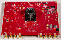
Cadence, a fabless semiconductor company focusing on the development of IP solutions and IC design and verification tools, today posted an update regarding their development efforts for the 5th generation of DDR memory which is giving us some insights into the development of a new standard. The new DDR5 standard is supposed to bring better speeds and lower voltages while being more power-efficient. In the Cadence's blog called Breakfast Bytes, one of Cadence's memory experts talked about developments of the new standards and how they are developing the IP for the upcoming SoC solutions. Even though JEDEC, a company developing memory standards, hasn't officially published DDR5 standard specifications, Cadence is working closely with them to ensure that they stay on track and be the first on the market to deliver IP for the new standard.

Marc Greenberg, a Cadence expert for memory solutions was sharing his thoughts in the blog about the DDR5 and how it is progressing. Firstly, he notes that DDR5 is going to feature 4800 MT/s speeds at first. The initial speeds will improve throughout the 12 months when the data transfer rate will increase in the same fashion we have seen with previous generation DDR standards. Mr. Greenberg also shared that the goals of DDR5 are to have larger memory dies while managing latency challenges, same speed DRAM core as DDR4 with a higher speed I/O. He also noted that the goal of the new standard is not the bandwidth, but rather capacity - there should be 24Gb of memory per die initially, while later it should go up to 32Gb. That will allow for 256 GB DIMMs, where each byte can be accessed under 100 ns, making for a very responsive system. Mr. Greenberg also added that this is the year of DDR5, as Cadence is receiving a lot of orders for their 7 nm IP which should go in production systems this year.
Cadence DDR5

Micron to Launch HBM2 Memory This Year

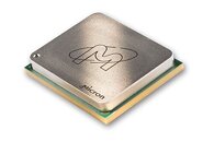
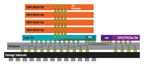
Micron Technologies, in the latest earnings report, announced that they will start shipping High-Bandwidth Memory 2 (HBM2) DRAM. Used for high-performance graphics cards, server processors and all kinds of processors, HBM2 memory is wanted and relatively expensive solution, however, when Micron enters the market of its manufacturing, prices, and the market should adjust for the new player. Previously, only SK-Hynix and Samsung were manufacturing the HBM2 DRAM, however, Micron will join them and they will again form a "big-three" pact that dominates the memory market.

Up until now, Micron used to lay all hopes on its proprietary Hybrid Memory Cube (HMC) DRAM type, which didn't gain much traction from customers and it never really took off. Only a few rare products used it, as Fujitsu SPARC64 XIfx CPU used in Fujitsu PRIMEHPC FX100 supercomputer introduced in 2015. Micron announced to suspend works on HMC in 2018 and decided to devote their efforts to GDDR6 and HBM development. So, as a result, we are seeing that they will launch HBM2 DRAM products sometime this year.
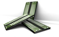
Micron HMC High-Bandwidth Memory

Samsung Announces Industry's First EUV DRAM with Shipment of First Million Modules

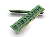
Samsung Electronics Co., Ltd., the world leader in advanced memory technology, today announced that it has successfully shipped one million of the industry's first 10 nm-class (D1x) DDR4 (Double Date Rate 4) DRAM modules based on extreme ultraviolet (EUV) technology. The new EUV-based DRAM modules have completed global customer evaluations, and will open the door to more cutting-edge EUV process nodes for use in premium PC, mobile, enterprise server and datacenter applications.

"With the production of our new EUV-based DRAM, we are demonstrating our full commitment toward providing revolutionary DRAM solutions in support of our global IT customers," said Jung-bae Lee, executive vice president of DRAM Product & Technology at Samsung Electronics. "This major advancement underscores how we will continue contributing to global IT innovation through timely development of leading-edge process technologies and next-generation memory products for the premium memory market."
Samsung EUV DDR4

Micron Samples the Industry's First uMCP Product With LPDDR5 to Increase Performance and Battery Life in 5G Smartphones

Micron Technology, Inc., today announced it began sampling the industry's first universal flash storage (UFS) multichip package (uMCP) with low-power DDR5 (LPDDR5) DRAM. The uMCP provides high-density and low-power storage designed to fit on slim and compact midrange smartphone designs.

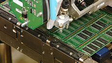
Micron's new uMCP5 packaging builds on the company's innovation and leadership in multichip form factors. Micron uMCPs combine low-power DRAM with NAND and an onboard controller, using 40% less space compared to a two-chip solution. This optimized configuration saves power, reduces memory footprint and enables smaller and more agile smartphone designs.
RAM Production

Ampere Computing Uncovers 80 Core "Cloud-Native" Arm Processor

Ampere Computing, a startup focusing on making HPC and processors from cloud applications based on Arm Instruction Set Architecture, today announced the release of a first 80 core "cloud-native" processor based on the Arm ISA. The new Ampere Altra CPU is the company's first 80 core CPU meant for hyper scalers like Amazon AWS, Microsoft Azure, and Google Cloud. Being built on TSMC's 7 nm semiconductor manufacturing process, the Altra is a CPU that is utilizing a monolithic die to achieve maximum performance. Using Arm's v8.2+ instruction set, the CPU is using the Neoverse N1 platform as its core, to be ready for any data center workload needed. It also borrows a few security features from v8.3 and v8.5, namely the hardware mitigations of speculative attacks.
When it comes to the core itself, the CPU is running at 3.0 GHz frequency and has some very interesting specifications. The design of the core is such that it is 4-wide superscalar Out of Order Execution (OoOE), which Ampere refers to as "aggressive" meaning that there is a lot of data throughput going on. The cache levels are structured in a way that there is 64 KB of L1D and L1I cache per core, along with 1 MB of L2 cache per core as well. For system-level cache, there is 32 MB of L3 available to the SoC. All of the caches have Error-correcting code (ECC) built-in, giving the CPU a much-needed feature. There are two 128-bit wide Single Instruction Multiple Data (SIMD) units, which are there to do parallel processing if needed. There is no mention if they implement Arm's Scalable Vector Extensions (SVE) or not.

Europe Readies its First Prototype of Custom HPC Processor

European Processor Initiative (EPI) is a Europe's project to kickstart a homegrown development of custom processors tailored towards different usage models that the European Union might need. The first task of EPI is to create a custom processor for high-performance computing applications like machine learning, and the chip prototypes are already on their way. The EPI chairman of the board Jean-Marc Denis recently spoke to the Next Platform and confirmed some information regarding the processor design goals and the timeframe of launch.

Supposed to be manufactured on TSMC's 6 nm EUV (TSMC N6 EUV) technology, the EPI processor will tape-out at the end of 2020 or the beginning of 2021, and it is going to be heterogeneous. That means that on its 2.5D die, many different IPs will be present. The processor will use a custom ARM CPU, based on a "Zeus" iteration of Neoverese server core, meant for general-purpose computation tasks like running the OS. When it comes to the special-purpose chips, EPI will incorporate a chip named Titan - a RISC-V based processor that uses vector and tensor processing units to compute AI tasks. The Titan will use every new standard for AI processing, including FP32, FP64, INT8, and bfloat16. The system will use HBM memory allocated to the Titan processor, have DDR5 links for the CPU, and feature PCIe 5.0 for the inner connection.

Intel's Frost Canyon NUC 10 Mini PC is now Available

Intel's latest NUC (Next Unit of Computing) series of Mini PCs, based on the 10th generation of Intel "Core" processors, is now available for purchase. Dubbed Frost Canyon, this NUC series is featuring Intel's 10th generation Comet Lake CPUs at its base. All of the available configurations are based around the Intel Core i7-10710U processor, Intel i219-V Gigabit Lan, Bluetooth 5.0 and Intel WiFi 6 AX200 networking module. Configurations are varying by the amount of pre-installed RAM and storage and the option of whatever you want OS pre-installed or not.

The NUC 10 supports up to 64 GB of DDR4 memory, while the storage options include space for one 2.5 inch SSD/HDD in smaller variants or two 2.5 inch SSD/HDD drives in taller variants, with one NVMe M.2 SSD slot available in both versions. Pricing starts at $679 for the base models, while higher-end configurations cost upward of $1,295. Additionally, it is worth pointing out that all CPUs inside the new NUC are configured to run at 25 W of TPD, regardless of the model. This will result in higher performance compared to 15 W versions of processors found in most laptop solutions.

ADATA Launches High-Capacity XPG Hunter DDR4 Modules

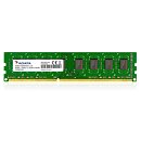
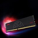
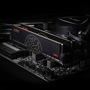
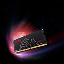
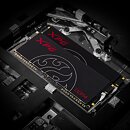
ADATA Technology, a leading manufacturer of high-performance DRAM modules, NAND Flash products, and mobile accessories today announces the launch of the XPG Hunter DDR4 memory module. Geared toward PC enthusiasts and gamers, the XPG Hunter delivers all the benefits of DDR4 with remarkable performance and efficiency. It supports XMP 2.0 for easy overclocking and offers great stability, making it ideal for performance seekers - gaming to competitive benchmarking. It comes in U-DIMM and SO-DIMM variants to meet the needs of desktop and notebook users alike.

The XPG Hunter modules are made with high-quality chips selected through a strict filtering process. They are equipped with the finest PCBs and pass rigid reliability and compatibility tests to ensure longevity and rugged durability, which are vital for overclocking, gaming, and extreme benchmarking. The modules deliver high-speed performance of up to 3200 MHz and comes with capacities of 4 GB, 8 GB, 16 GB, or 32 GB to meet the needs of diverse users and budgets.

ChangXin Becomes China's First Domestic DRAM Supplier

ChangXin Memory Technologies, a Chinese startup founded in 2016 that was formerly known as "Innotron Memory", now claims that it has become China's first and only domestic DRAM supplier. Following the announcement that it started production of domestic DRAM chips, ChangXin is now reportedly shipping its first DRAM wafers. With an output of around 20000 wafers per month, the company is currently building LPDDR4, DDR4 8Gbit chips using the "10-nanometer class" node, which is supposed to be 18 or 19 nm size in reality.

The company expects to double its wafer output to 40000 wafers per month sometime around Q2 of 2020 when additional expansion facilities will start production. ChangXin plans to soon open two more manufacturing facilities to start manufacturing even more wafers, in addition to its Fab 1. So far ChangXin has laid-out plans to start manufacturing DRAM technology based on stack capacitor, which is different from the usual trench capacitor technology few companies are pursuing.

ASRock Announces Brand new Mars Series of Mini PCs

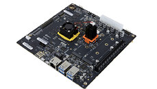
The leading global motherboard & graphics card manufacturer, ASRock, a pleasure to launch brand new compact Mini PC - Mars Series. Supports up to Intel Core i5 Quad-Core processor, 32 GB DDR4-2666 MHz, PCIe NVMe M.2 SSD, 2.5-inch hard drive, and wireless connectivity; all implies into 0.7-liter chassis with 26 mm height.

ASRock Mars offers abundant USB devices connectivity, features a total of 7 USB ports, including one Type-C port; In addition, the native SD card reader and dual display outputs to provide more productive and convenience.

Samsung Starts Offering First A-Die Based RAM

Samsung's B die has been widely known as a good, high performance variant of DRAM memory, loved by overclockers because of its ability to get to a high frequency with relatively low timings. However, B die has been discontinued and now Samsung started offering its replacement in form of the newly developed A die manufactured in 1z nm (1z class) lithography process. Despite the lack of technical details surrounding the new die type, Hardwareluxx has received a tip from its reader about new RAM offering that incorporates A die memory.

The M378A4G43AB2-CVF, as it is called in the listing, is a 32 GB, single dimm DDR4 RAM with operating speed of 2933 MHz and CL21-21-21 timings. This particular offer isn't something to be excited about as the frequency is good, but the timings are quite high for that speed. Given that we don't know where the A die is targeted at, we can speculate that its current aim is at mid-tier systems, where the mediocre performance is okay and the system isn't suffering (performance wise) because of it. Nonetheless this find is quite interesting as it gives first hints at what can we expect in therms of future A die DRAM offerings. Remember, it took some time for B die as well to get to the level of performance we have today, so it is entirely possible that A die will improve and try to aim for greater performance level than it currently has.

Micron Commences Volume Production of 1z Nanometer DRAM Process Node

Micron Technology, Inc. (Nasdaq: MU), today announced advancements in DRAM scaling, making Micron the first memory company to begin mass production of 16 Gb DDR4 products using 1z nm process technology

"Development and mass production of the industry's smallest feature size DRAM node are a testament to Micron's world-class engineering and manufacturing capabilities, especially at a time when DRAM scaling is becoming extremely complex," said Scott DeBoer, executive vice president of Technology Development for Micron Technology. "Being first to market strongly positions us to continue offering high-value solutions across a wide portfolio of end customer applications."

Intel Starts Shipping 10 nm Ice Lake CPUs to OEMs

During its second quarter earnings call, Intel announced that it has started shipping of 10th generation "Core" CPUs to OEMs. Making use of 10 nm lithography, the 10th generation of "Core" CPUs, codenamed Ice Lake, were qualified by OEMs earlier in 2019 in order to be integrated into future products. Ice Lake is on track for holiday season 2019, meaning that we can expect products on-shelves by the end of this year. That is exciting news as the 10th generation of Core CPUs is bringing some exciting micro-architectural improvements along with the long awaited and delayed Intel's 10nm manufacturing process node.

The new CPUs are supposed to get around 18% IPC improvement on average when looking at direct comparison to previous generation of Intel CPUs, while being clocked at same frequency. This time, even regular mobile/desktop parts will get AVX512 support, alongside VNNI and Cryptography ISA extensions that are supposed to bring additional security and performance for the ever increasing number of tasks, especially new ones like Neural Network processing. Core configurations will be ranging from dual core i3 to quad core i7, where we will see total of 11 models available.

G.SKILL Announces OC World Cup 2019 Competition

G.SKILL International Enterprise Co., Ltd., the world's leading manufacturer of extreme performance memory and gaming peripherals, is excited to announce the 6th Annual OC World Cup 2019. The online qualifier competition stage will be held from March 13, 2019 until April 16, 2019 on hwbot.org. The top 9 winners of the online qualifier will be qualified to join the live competition at the G.SKILL booth during Computex 2019 week from May 29th to 31st and compete for a chunk of the $25,000 USD cash prize pool.

With the participation of top overclockers from around the world and carefully designed rules, G.SKILL OC World Cup is considered as one of the most challenging overclocking competition by professional overclockers. The G.SKILL OC World Cup consists of three rounds: Online Qualifier, Live Qualifier, and Grand Final. The top 9 winners of the Online Qualifier will receive eligibility to enter the Live Qualifier stage during Computex 2019 and demonstrate their finest LN2 extreme overclocking skills at the G.SKILL booth.

Samsung Ready with 32GB DDR4 UDIMMs for Desktops, Paving the Way for 16GB Single-Rank

Samsung is ready with a 32 GB DDR4 UDIMM (unbuffered DIMMs) targeted at desktops. Dual-channel kits with these modules could let you max out the 64 GB memory limit of today's mainstream desktop processors, and 128 GB limits of Intel's Core X HEDT processors, with quad-channel kits. AMD's Ryzen Threadripper processors are advertised to support up to 2 TB of memory (including ECC support), so it should finally be possible to pack up to 256 GB of memory on Threadripper-powered machines.

The new M378A4G43MB1-CTD DDR4 UDIMM from Samsung is, unsurprisingly, a dual-rank module (x8 / x16 Organization or up to 2 ranks per DIMM and 2DPC configuration). It ticks at DDR4-2666 at a module voltage of 1.2 V. The module itself won't be much to look at, with a green PCB and bare-naked DRAM chips. It is is currently sampling to PC OEMs. It could also be possible for more popular memory manufacturers to get in touch with Samsung for the DRAM chips that make up this module. A single-rank variant of this module could finally make it possible for AMD Ryzen AM4 machines to have 32 GB of dual-channel memory at acceptably high memory clocks.

NVIDIA "TU102" RT Core and Tensor Core Counts Revealed

The GeForce RTX 2080 Ti is indeed based on an ASIC codenamed "TU102." NVIDIA was referring to this 775 mm² chip when talking about the 18.5 billion-transistor count in its keynote. The company also provided a breakdown of its various "cores," and a block-diagram. The GPU is still laid out like its predecessors, but each of the 72 streaming multiprocessors (SMs) packs RT cores and Tensor cores in addition to CUDA cores.

The TU102 features six GPCs (graphics processing clusters), which each pack 12 SMs. Each SM packs 64 CUDA cores, 8 Tensor cores, and 1 RT core. Each GPC packs six geometry units. The GPU also packs 288 TMUs and 96 ROPs. The TU102 supports a 384-bit wide GDDR6 memory bus, supporting 14 Gbps memory. There are also two NVLink channels, which NVIDIA plans to later launch as its next-generation multi-GPU technology.

NAND Flash Supply to Improve in 1Q18

DigiTimes, quoting industry sources, reports that NAND flash supply should see improvements from its 4Q17 state in 2018. This likely doesn't come as much of a surprise - 2017 has been a sort of "squeeze" year for NAND and DDR memory manufacturing, with companies increasing production without committing to fully satisfy demand, which in turn translates to longer term higher pricing of memory. Still, those tentative increases to production capabilities should begin to release the memory pricing squeeze during 1Q18, with ASP (average selling price) coming down.

The increase in production and supply doesn't come solely from factory floor expansions, however; there's also been reports of increased yields of 3D NAND fabrication technologies, which should also increase availability in the best way possible for manufacturers.
Return to Keyword Browsing
Nov 21st, 2024 11:54 EST change timezone

New Forum Posts

Popular Reviews

Controversial News Posts