News Posts matching #EPYC

Return to Keyword Browsing

AMD "Matisse" and "Rome" IO Controller Dies Mapped Out

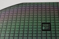
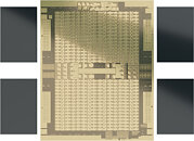
Here are the first detailed die maps of the I/O controller dies of AMD's "Matisse" and "Rome" multi-chip modules that make up the company's 3rd generation Ryzen and 2nd generation EPYC processor families, respectively, by PC enthusiast and VLSI engineer "Nemez" aka @GPUsAreMagic on Twitter, with underlying die-shots by Fitzchens Fitz. The die maps of the "Matisse" cIOD in particular give us fascinating insights to how AMD designed the die to serve both as a cIOD and as an external FCH (AMD X570 and TRX40 chipsets). At the heart of both these chips' design effort is using highly configurable SerDes (serializer/deserializers) that can work as PCIe, SATA, USB 3, or other high-bandwidth serial interfaces, using a network of fabric switches and PHYs. This is how motherboard designers are able to configure the chipsets for the I/O they want for their specific board designs.

The "Matisse" cIOD has two x16 SerDes controllers and an I/O root hub, along with two configurable x16 SerDes PHYs, while the "Rome" sIOD has four times as many SerDes controllers, along with eight times as many PHYs. The "Castle Peak" cIOD (3rd gen Ryzen Threadripper) disables half the SerDes resources on the "Rome" sIOD, along with half as many memory controllers and PHYs, limiting it to 4-channel DDR4. The "Matisse" cIOD features two IFOP (Infinity Fabric over Package) links, wiring out to the two "Zen 2" CCDs (chiplets) on the MCM, while the "Rome" sIOD features eight such IFOP interfaces for up to eight CCDs, along with IFIS (Infinity Fabric Inter-Socket) links for 2P motherboards. Infinity Fabric internally connects all components on both IOD dies. Both dies are built on the 12 nm FinFET (12LP) silicon fabrication node at GlobalFoundries.
Matisse cIOD Rome cIOD

TYAN Updates Transport HX Barebones with New AMD EPYC 7002 Series Processors

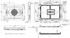
TYAN, an industry-leading server platform design manufacturer and MiTAC Computing Technology Corporation subsidiary, today announced support for high frequency AMD EPYC 7F32, AMD EPYC 7F52 and AMD EPYC 7F72 processor-based server motherboards and server systems to the market. TYAN's HPC and storage server platforms continue to offer exceptional performance to datacenter customers.
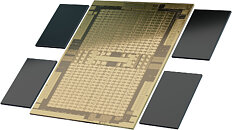
"Leveraging AMD's innovation in 7 nm process technology, PCIe 4.0 I/O, and an embedded security architecture, TYAN's 2nd Gen AMD EPYC processor-based platforms are designed to address the most demanding challenges facing the datacenter", said Danny Hsu, Vice President of MiTAC Computing Technology Corporation's TYAN Business Unit. "Adding the new AMD EPYC 7002 Series processors with TYAN server platforms enable us to provide new capabilities to our customers and partners."

x86 Lacks Innovation, Arm is Catching up. Enough to Replace the Giant?

Intel's x86 processor architecture has been the dominant CPU instruction set for many decades, since IBM decided to put the Intel 8086 microprocessor into its first Personal Computer. Later, in 2006, Apple decided to replace their PowerPC based processors in Macintosh computers with Intel chips, too. This was the time when x86 became the only option for the masses to use and develop all their software on. While mobile phones and embedded devices are mostly Arm today, it is clear that x86 is still the dominant ISA (Instruction Set Architecture) for desktop computers today, with both Intel and AMD producing processors for it. Those processors are going inside millions of PCs that are used every day. Today I would like to share my thoughts on the demise of the x86 platform and how it might vanish in favor of the RISC-based Arm architecture.

Both AMD and Intel as producer, and millions of companies as consumer, have invested heavily in the x86 architecture, so why would x86 ever go extinct if "it just works"? The answer is that it doesn't just work.

AMD Financial Analyst Day 2020 Live Blog

AMD Financial Analyst Day presents an opportunity for AMD to talk straight with the finance industry about the company's current financial health, and a taste of what's to come. Guidance and product teasers made during this time are usually very accurate due to the nature of the audience. In this live blog, we will post information from the Financial Analyst Day 2020 as it unfolds.
20:59 UTC: The event has started as of 1 PM PST. CEO Dr Lisa Su takes stage.

AMD Scores Another EPYC Win in Exascale Computing With DOE's "El Capitan" Two-Exaflop Supercomputer

AMD has been on a roll in both consumer, professional, and exascale computing environments, and it has just snagged itself another hugely important contract. The US Department of Energy (DOE) has just announced the winners for their next-gen, exascale supercomputer that aims to be the world's fastest. Dubbed "El Capitan", the new supercomputer will be powered by AMD's next-gen EPYC Genoa processors (Zen 4 architecture) and Radeon GPUs. This is the first such exascale contract where AMD is the sole purveyor of both CPUs and GPUs, with AMD's other design win with EPYC in the Cray Shasta being paired with NVIDIA graphics cards.

El Capitan will be a $600 million investment to be deployed in late 2022 and operational in 2023. Undoubtedly, next-gen proposals from AMD, Intel and NVIDIA were presented, with AMD winning the shootout in a big way. While initially the DOE projected El Capitan to provide some 1.5 exaflops of computing power, it has now revised their performance goals to a pure 2 exaflop machine. El Capitan willl thus be ten times faster than the current leader of the supercomputing world, Summit.

Cloudflare Deploys AMD EPYC Processors Across its Latest Gen X Servers

The ubiquitous DDoS-mitigation and CDN provider, Cloudflare, announced that its latest Gen X servers implement AMD EPYC processors ditching Intel Xeons with its older Gen 9 servers. Cloudflare uses multi-functional servers (just like Google), in which each server is capable of handling any kind of the company's workloads (DDoS mitigation, content delivery, DNS, web-security, etc.). The company minimizes server hardware configurations so they're easier to maintain and lower TCO. The hardware specs of its servers are periodically updated and classified by "generations."

Cloudflare's Gen X server is configured with a single-socket 2nd gen AMD EPYC 7642 processor (48-core/96-thread, 256 MB L3 cache), and 256 GB of octa-channel DDR4-2933 memory, along with NVMe flash-based primary storage. "We selected the AMD EPYC 7642 processor in a single-socket configuration for Gen X. This CPU has 48-cores (96 threads), a base clock speed of 2.4 GHz, and an L3 cache of 256 MB. While the rated power (225 W) may seem high, it is lower than the combined TDP in our Gen 9 servers and we preferred the performance of this CPU over lower power variants. Despite AMD offering a higher core count option with 64-cores, the performance gains for our software stack and usage weren't compelling enough," Cloudflare writes in its blog post announcing Gen X. The new servers will go online in the coming weeks.
Many Thanks to biffzinker for the tip.

KIOXIA First to Deliver Enterprise and Data Center PCIe 4.0 U.3 SSDs

The PCI Express 4.0 specification was designed to double the performance of server and storage systems, pushing speeds up to 16.0 gigatransfers per second (GT/s) or 2 gigabits per second (Gb/s) throughput per lane, and driving new performance levels for cloud and enterprise applications. Today, KIOXIA America, Inc. (formerly Toshiba Memory America, Inc.) announced that its lineup of CM6 and CD6 Series PCIe 4.0 NVM Express (NVMe ) enterprise and data center solid state drives (SSDs) are now shipping to customers.

An established leader in developing PCIe and NVMe SSDs, KIOXIA delivers never-before-seen performance. KIOXIA was the first company to publicly demonstrate PCIe 4.0 SSDs and is now the first to ship these next-generation drives. The CM6 and CD6 Series SSDs are compliant to the latest NVMe specification, and include key features such as in-band NVMe-MI, persistent event log, namespace granularity, and shared stream writes. Additionally, both drives are SFF-TA-1001 conformant (also known as U.3), which allows them to be used in tri-mode enabled backplanes, which can accept SAS, SATA or NVMe SSDs.

AMD Gets Design Win in Cray Shasta Supercomputer for US Navy DSRC With 290,304 EPYC Cores

AMD has scored yet another design win for usage of its high-performance EPYC processors in the Cray Shasta supercomputer. The Cray Shasta will be deployed in the US Navy's Department of Defense Supercomputing Resource Center (DSRC) as part of the High Performance Computing Modernization Program. The peak theoretical computing capability of 12.8 PetaFLOPS, or 12.8 quadrillion floating point operations per second supercomputer will be built with 290,304 AMD EPYC (Rome) processor cores and 112 NVIDIA Volta V100 General-Purpose Graphics Processing Units (GPGPUs). The system will also feature 590 total terabytes (TB) of memory and 14 petabytes (PB) of usable storage, including 1 PB of NVMe-based solid state storage. Cray's Slingshot network will make sure all those components talk to each other at a rate of 200 Gigabits per second.

Navy DSRC supercomputers support climate, weather, and ocean modeling by NMOC, which assists U.S. Navy meteorologists and oceanographers in predicting environmental conditions that may affect the Navy fleet. Among other scientific endeavors, the new supercomputer will be used to enhance weather forecasting models; ultimately, this improves the accuracy of hurricane intensity and track forecasts. The system is expected to be online by early fiscal year 2021.

VMWare Updates Licensing Model, Setting 32-Core Limit per License

VMWare, one of the most popular virtualization solutions commercially available for businesses and the industry in general, has announced changes to its licensing model. From now on, licensees will have to acquire a license per 32 CPU cores, instead of the former "per socket" model. This effectively means that users who had made a migration to AMD's 64-core EPYC CPUs, for instance, and who saved on both price-per core and VMWare licensing fees compared to Intel customers (who would need two sockets to achieve the same core-count, and thus, two licenses) are now being charged for two licenses for a 64-core, AMD-populated socket. This was a selling point for AMD - the company stated that their high-end EPYC processors could act as a dual-socket setup with a single processor, thanks to EPYC's I/O capabilities and core counts. VMWare claims this change is in line with industry standard pricing models.

Of course this decision from VMWare hits AMD the hardest, and it comes at a time where there are already 48 and 64 core CPUs available in the market. Should this licensing change be done, perhaps it should be in line with the current state of the industry, and not following in a quasi-random core-count (it definitely isn't random, though, and I'll leave it at that). From VMware's perspective, AMD's humongous CPU core counts does affect their bottom line. The official release claiming customers license software based on CPU counts may be valid, and they do allow for free licenses for servers past 32 cores until April 30, 2020. Of course, VMWare is also preparing itself for future industry changes - Intel will obviously increase its core counts in response to AMD's EPYC attack on the expected core counts of professional applications.

NVIDIA's Next-Generation "Ampere" GPUs Could Have 18 TeraFLOPs of Compute Performance

NVIDIA will soon launch its next-generation lineup of graphics cards based on a new and improved "Ampere" architecture. With the first Tesla server cards that are a part of the Ampere lineup going inside Indiana University Big Red 200 supercomputer, we now have some potential specifications and information about its compute performance. Thanks to the Twitter user dylan552p(@dylan522p), who did some math about the potential compute performance of the Ampere GPUs based on NextPlatform's report, we discovered that Ampere is potentially going to feature up to 18 TeraFLOPs of FP64 compute performance.

With Big Red 200 supercomputer being based on Cray's Shasta supercomputer building block, it is being deployed in two phases. The first phase is the deployment of 672 dual-socket nodes powered by AMD's EPYC 7742 "Rome" processors. These CPUs provide 3.15 PetaFLOPs of combined FP64 performance. With a total of 8 PetaFLOPs planned to be achieved by the Big Red 200, that leaves just a bit under 5 PetaFLOPs to be had using GPU+CPU enabled system. Considering the configuration of a node that contains one next-generation AMD "Milan" 64 core CPU, and four of NVIDIA's "Ampere" GPUs alongside it. If we take for a fact that Milan boosts FP64 performance by 25% compared to Rome, then the math shows that the 256 GPUs that will be delivered in the second phase of Big Red 200 deployment will feature up to 18 TeraFLOPs of FP64 compute performance. Even if "Milan" doubles the FP64 compute power of "Rome", there will be around 17.6 TeraFLOPs of FP64 performance for the GPU.

AMD Strengthens Senior Leadership Team

AMD (NASDAQ: AMD) today announced several promotions and a new hire to strengthen its senior leadership team to further enable the company's continued growth.

AMD announced four senior vice president promotions:
  • Nazar Zaidi to senior vice president of Cores, Server SoC and Systems IP Engineering with continued responsibility for leading the development of leadership CPU cores, server SoCs and system IP.
  • Andrej Zdravkovic to senior vice president of Software Development, leading the teams responsible for all aspects of AMD software strategy and development across AMD graphics, client and data center products.
  • Spencer Pan to senior vice president of Greater China Sales and president of AMD Greater China, with responsibility for leading all sales and go-to-market activities for AMD in Greater China and expansion of strategic partner and customer relationships in the region.
  • Jane Roney to senior vice president of Business Operations, responsible for aligning and scaling critical business processes across the company to support growth and help ensure consistent execution.

AMD CEO To Unveil "Zen 3" Microarchitecture at CES 2020

A prominent Taiwanese newspaper reported that AMD will formally unveil its next-generation "Zen 3" CPU microarchitecture at the 2020 International CES. Company CEO Dr Lisa Su will head an address revealing three key client-segment products under the new 4th generation Ryzen processor family, and the company's 3rd generation EPYC enterprise processor family based on the "Milan" MCM that succeeds "Rome." AMD is keen on developing an HEDT version of "Milan" for the 4th generation Ryzen Threadripper family, codenamed "Genesis Peak."

The bulk of the client-segment will be addressed by two distinct developments, "Vermeer" and "Renoir." The "Vermeer" processor is a client-desktop MCM that succeeds "Matisse," and will implement "Zen 3" chiplets. "Renoir," on the other hand, is expected to be a monolithic APU that combines "Zen 2" CPU cores with an iGPU based on the "Vega" graphics architecture, with updated display- and multimedia-engines from "Navi." The common thread between "Milan," "Genesis Peak," and "Vermeer" is the "Zen 3" chiplet, which AMD will build on the new 7 nm EUV silicon fabrication process at TSMC. AMD stated that "Zen 3" will have IPC increases in line with a new microarchitecture.

AMD Reports Third Quarter 2019 Financial Results

AMD (NASDAQ:AMD) today announced revenue for the third quarter of 2019 of $1.80 billion, operating income of $186 million, net income of $120 million and diluted earnings per share of $0.11. On a non-GAAP(*) basis, operating income was $240 million, net income was $219 million and diluted earnings per share was $0.18.

"Our first full quarter of 7 nm Ryzen, Radeon and EPYC processor sales drove our highest quarterly revenue since 2005, our highest quarterly gross margin since 2012 and a significant increase in net income year-over-year," said Dr. Lisa Su, AMD president and CEO. "I am extremely pleased with our progress as we have the strongest product portfolio in our history, significant customer momentum and a leadership product roadmap for 2020 and beyond."

AMD Zen 3 Could Bid the CCX Farewell, Feature Updated SMT

With its next-generation "Zen 3" CPU microarchitecture designed for the 7 nm EUV silicon fabrication process, AMD could bid the "Zen" compute complex or CCX farewell, heralding chiplets with monolithic last-level caches (L3 caches) that are shared across all cores on the chiplet. AMD embraced a quad-core compute complex approach to building multi-core processors with "Zen." At the time, the 8-core "Zeppelin" die featured two CCX with four cores, each. With "Zen 2," AMD reduced the CPU chiplet to only containing CPU cores, L3 cache, and an Infinity Fabric interface, talking to an I/O controller die elsewhere on the processor package. This reduces the economic or technical utility in retaining the CCX topology, which limits the amount of L3 cache individual cores can access.

This and more juicy details about "Zen 3" were put out by a leaked (later deleted) technical presentation by company CTO Mark Papermaster. On the EPYC side of things, AMD's design efforts will be spearheaded by the "Milan" multi-chip module, featuring up to 64 cores spread across eight 8-core chiplets. Papermaster talked about how the individual chiplets will feature "unified" 32 MB of last-level cache, which means a deprecation of the CCX topology. He also detailed an updated SMT implementation that doubles the number of logical processors per physical core. The I/O interface of "Milan" will retain PCI-Express gen 4.0 and eight-channel DDR4 memory interface.

AMD Could Release Next Generation EPYC CPUs with Four-Way SMT

AMD has completed design phase of its "Zen 3" architecture and rumors are already appearing about its details. This time, Hardwareluxx has reported that AMD could bake a four-way simultaneous multithreading technology in its Zen 3 core to enable more performance and boost parallel processing power of its data center CPUs. Expected to arrive sometime in 2020, Zen 3 server CPUs, codenamed "MILAN", are expected to bring many architectural improvements and make use of TSMC's 7nm+ Extreme Ultra Violet lithography that brings as much as 20% increase in transistor density.

Perhaps the biggest change we could see is the addition of four-way SMT that should allow a CPU to have four virtual threads per core that will improve parallel processing power and enable data center users to run more virtual machines than ever before. Four-way SMT will theoretically boost performance by dividing micro-ops into four smaller groups so that each thread could execute part of the operation, thus making the execution time much shorter. This being only one application of four-way SMT, we can expect AMD to leverage this feature in a way that is most practical and brings the best performance possible.

2nd Gen AMD EPYC Continues Market Momentum with New Customers

At the European launch in Rome, Italy AMD today highlighted the growing adoption of 2nd Gen AMD EPYC processors across cloud, enterprise and HPC customers. "Today, we are proud to have new platforms from Dell and new customers adopting 2nd Gen AMD EPYC for cloud, enterprise computing and HPC," said Forrest Norrod, senior vice president and general manager, Datacenter and Embedded Solutions Business Group. "We continue to take the AMD EPYC processor to new heights and are thrilled to have the ecosystem supporting us across hardware, software and cloud providers as we face the challenges of the modern data center head-on."

AMD also announced a new addition to the 2nd Generation AMD EPYC family, the AMD EPYC 7H12 processor. The 64 core/128 thread, 2.60 GHz base frequency, 3.30 GHz max boost frequency, 280 W TDP processor is specifically built for HPC customers and workloads, using liquid cooling to deliver leadership supercomputing performance. In an ATOS testing on their BullSequana XH2000, the new AMD EPYC 7H12 processor achieved a LINPACK score of ~ 4.2 TeraFLOPS, ~11% better than the AMD EPYC 7742 processor.

AMD Readies Three HEDT Chipsets: TRX40, TRX80, and WRX80

AMD is preparing to surprise Intel with its 3rd generation Ryzen Threadripper processors derived from the "Rome" MCM (codenamed "Castle Peak" for the client-platform), that features up to 64 CPU cores, a monolithic 8-channel DDR4 memory interface, and 128 PCIe gen 4.0 lanes. For the HEDT platform, AMD could reconfigure the I/O controller die for two distinct sub-platforms within HEDT - one targeting gamers/enthusiasts, and another targeting the demographic that buys Xeon W processors, including the W-3175X. The gamer/enthusiast-targeted processor line could feature a monolithic 4-channel DDR4 memory interface, and 64 PCI-Express gen 4.0 lanes from the processor socket, and additional lanes from the chipset; while the workstation-targeted processor line could essentially be EPYCs, with a wider memory bus width and more platform PCIe lanes; while retaining drop-in backwards-compatibility with AMD X399 (at the cost of physically narrower memory and PCIe I/O).

To support this diverse line of processors, AMD is coming up with not one, but three new chipsets: TRX40, TRX80, and WRX80. The TRX40 could have a lighter I/O feature-set (similar to the X570), and probably 4-channel memory on the motherboards. The TRX80 and WRX80 could leverage the full I/O of the "Rome" MCM, with 8-channel memory and more than 64 PCIe lanes. We're not sure what differentiates the TRX80 and WRX80, but we believe motherboards based on the latter will resemble proper workstation boards in form-factors such as SSI, and be made by enterprise motherboard manufacturers such as TYAN. The chipsets made their way to the USB-IF for certification, and were sniffed out by momomo_us. ASUS is ready with its first motherboards based on the TRX40, the Prime TRX40-Pro, and the ROG Strix TRX40-E Gaming.

GIGABYTE Smashes 11 World Records with New AMD EPYC 7002 Processors

GIGABYTE, a leading server systems builder which recently released a total of 17 new AMD EPYC 7002 Series "Rome" server platforms simultaneously with AMD's own official launch of their next generation CPU, is proud to announce that our new systems have already broken 11 different SPEC benchmark world records. These new world records have not only been achieved against results from all alternative processor based systems but even against competing vendor solutions using the same 2nd Generation AMD EPYC 7002 Series "Rome" processor platform, illustrating that GIGABYTE's system design and engineering is perfectly optimized to deliver the maximum performance possible from the 2nd Generation AMD EPYC.

AMD "Sharkstooth" Shows Up on Geekbench: Possible Zen 2 Threadripper

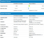
AMD is possibly testing its 3rd generation Ryzen Threadripper HEDT processors, with an interesting entry showing up on the Geekbench online database. The entry speaks of an "AMD Sharkstooth" processor with 32 cores and 64 threads, with a nominal clock speed of 3.60 GHz, and the long-form model number "AuthenticAMD Family 23 Model 49 Stepping 0." None of the 2nd generation EPYC processors correspond with these specs, and so we're almost certain this is a client-segment Ryzen Threadripper part.

The prototyping platform, which is a motherboard designed in-house by AMD to test the processor's various components and I/O capabilities, is codenamed "WhiteHavenOC-CP." In this Geekbench submission, the processor is paired with around 128 GB of memory, and tested on 64-bit Linux. The platform yields a multi-threaded score of 94,772 points, which is about 18.5 percent higher than what a Ryzen Threadripper 2990WX typically manages when tested on Linux. It is also within 5% of what the Xeon W-3175X manages (around 99,000 points). The production model could be clocked higher. AMD will also use the opportunity to launch a new motherboard chipset while maintaining backwards-compatibility with the AMD X399. This new chipset will enable PCI-Express gen 4.0 and come with stiffer CPU VRM and memory/PCIe wiring specifications to enable higher memory clocks and PCIe link stability. AMD is expected to launch its 3rd gen Ryzen Threadripper this October, to preempt Intel's next HEDT processor series.

Samsung PM1733 SSD and High-Density DIMMs Support AMD EPYC 7002 Series Processors

Samsung Electronics, Ltd., has taken its leadership position in the memory market a step further today by announcing support of the Samsung PM1733 PCIe Gen4 Solid State Drive (SSD) and high density RDIMM and LRDIMM dynamic random access memory (DRAM) for the AMD EPYC 7002 Generation Processors. AMD launched the 2nd Gen AMD EPYC processor in San Francisco yesterday.

"AMD has listened to the needs of its customers in developing the 2nd Gen AMD EPYC processors and has worked closely with us to integrate the best of our cutting-edge memory and storage products," said Jinman Han, senior VP of Memory Product Planning, Samsung Electronics. "With these new datacenter processors, AMD is providing customers with a processor that enables a new standard for the modern datacenter."

SK Hynix Named as Memory & Storage Solutions Partner to Support Latest AMD EPYC 7002 Series

SK Hynix Inc. announced today that its DRAM and Enterprise SSD (eSSD) solutions, including the up-to-date 1Y nm 8 Gb DDR4 DRAM, have been fully tested and validated with the new AMD EPYC 7002 Generation Processors, which were unveiled during AMD's launch event on August 7. The Company has worked closely with AMD to provide memory solutions fully compatible with the 2nd Gen AMD EPYC Processors, targeting high performance data centers.

The SK Hynix DDR4 DRAM supports the maximum speed of 3200 Mbps of the 2nd Gen EPYC Processors, which will increase memory performance more than 20% compared to the 1st Gen AMD EPYC Processors. The Company's various DDR4 DRAM solutions, based on the 1Xnm and 1Y nm technology with density of 8 Gb and 16 Gb, have been fully tested and validated with the 2nd Gen EPYC Processors. SK Hynix provides high-density DIMMs with density over 64 GB to support up to 64 cores per socket in the 2nd Gen EPYC.

SK Hynix also provides a full line-up of SATA and PCIe from 480 GB to 8 TB, which have also been validated and tested with the 2nd Gen EPYC. SK Hynix's eSSD solutions are optimized for the latest data center's read-intensive and mixed workload environment.

2nd Gen AMD EPYC Processors Set New Standard for the Modern Datacenter

At a launch event today, AMD was joined by an expansive ecosystem of datacenter partners and customers to introduce the 2nd Generation AMD EPYC family of processors that deliver performance leadership across a broad number of enterprise, cloud and high-performance computing (HPC) workloads. 2nd Gen AMD EPYC processors feature up to 64 "Zen 2" cores in leading-edge 7 nm process technology to deliver record-setting performance while helping reduce total cost of ownership (TCO) by up to 50% across numerous workloads. At the event, Google and Twitter announced new 2nd Gen AMD EPYC processor deployments and HPE and Lenovo announced immediate availability of new platforms.

"Today, we set a new standard for the modern datacenter with the launch of our 2nd Gen AMD EPYC processors that deliver record-setting performance and significantly lower total cost of ownership across a broad set of workloads," said Dr. Lisa Su, president and CEO, AMD. "Adoption of our new leadership server processors is accelerating with multiple new enterprise, cloud and HPC customers choosing EPYC processors to meet their most demanding server computing needs."

AMD Zen 2 EPYC "Rome" Launch Event Live Blog

AMD invited TechPowerUp to their launch event and editor's day coverage of Zen 2 EPYC processors based on the 7 nm process. The event was a day-long affair which included product demos and tours, and capped off with an official launch presentation which we are able to share with you live as the event goes on. Zen 2 with the Ryzen 3000-series processors ushered in a lot of excitement, and for good reason too as our own reviews show, but questions remained on how the platform would scale to the other end of the market. We already knew, for example, that AMD secured many contracts based on their first-generation EPYC processors, and no doubt the IPC increase and expected increased core count would cause similar, if not higher, interest here. We also expect to know shortly about the various SKUs and pricing involved, and also if AMD wants to shed more light on the future of the Threadripper processor family. Read below, and continue past the break, for our live coverage.
21:00 UTC: Lisa Su is on the stage at the Palace of Fine Arts events venue in San Francisco to present AMD's latest developments on EPYC for datacenters, using the Zen 2 microarchitecture.

21:10 UTC: AMD focuses not just on delivering a single chip, but it's goal is to deliver a complete solution for the enterprise.

Intel Internal Memo Reveals that even Intel is Impressed by AMD's Progress

Today an article was posted on Intel's internal employee-only portal called "Circuit News". The post, titled "AMD competitive profile: Where we go toe-to-toe, why they are resurgent, which chips of ours beat theirs" goes into detail about the recent history of AMD and how the company achieved its tremendous growth in recent years. Further, Intel talks about where they see the biggest challenges with AMD's new products, and what the company's "secret sauce" is to fight against these improvements.
The full article follows:

Intel "Sapphire Rapids" Brings PCIe Gen 5 and DDR5 to the Data-Center

As if the mother of all ironies, prior to its effective death-sentence dealt by the U.S. Department of Commerce, Huawei's server business developed an ambitious product roadmap for its Fusion Server family, aligning with Intel's enterprise processor roadmap. It describes in great detail the key features of these processors, such as core-counts, platform, and I/O. The "Sapphire Rapids" processor will introduce the biggest I/O advancements in close to a decade, when it releases sometime in 2021.

With an unannounced CPU core-count, the "Sapphire Rapids-SP" processor will introduce DDR5 memory support to the data-center, which aims to double bandwidth and memory capacity over the DDR4 generation. The processor features an 8-channel (512-bit wide) DDR5 memory interface. The second major I/O introduction is PCI-Express gen 5.0, which not only doubles bandwidth over gen 4.0 to 32 Gbps per lane, but also comes with a constellation of data-center-relevant features that Intel is pushing out in advance as part of the CXL Interconnect. CXL and PCIe gen 5 are practically identical.
Return to Keyword Browsing
Nov 21st, 2024 10:42 EST change timezone

New Forum Posts

Popular Reviews

Controversial News Posts