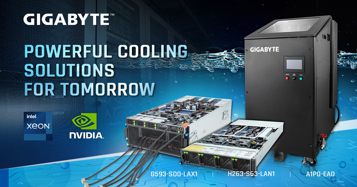
GIGABYTE Announces New Direct Liquid Cooling (DLC) Multi-Node Servers Ahead of SC23
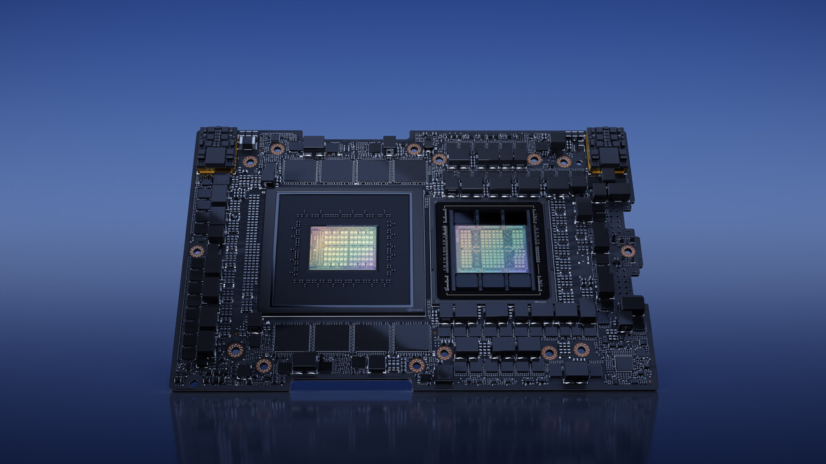
GIGABYTE Technology, Giga Computing, a subsidiary of GIGABYTE and an industry leader in high-performance servers, server motherboards, and workstations, today announced direct liquid cooling (DLC) multi-node servers for NVIDIA Grace CPU & NVIDIA Grace Hopper Superchip. In addition, a DLC ready Intel-based server for the NVIDIA HGX H100 8-GPU platform and a high-density server for AMD EPYC 9004 processors. For the ultimate in efficiency, is also a new 12U single-phase immersion tank. All these mentioned products will be at GIGABYTE booth #355 at SC23.
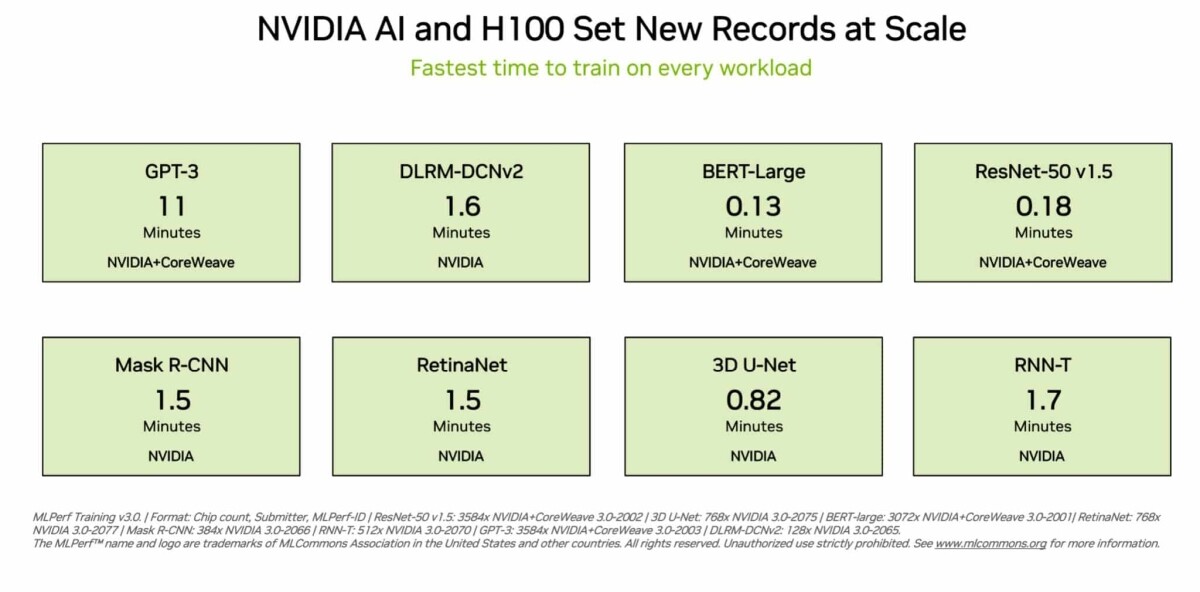
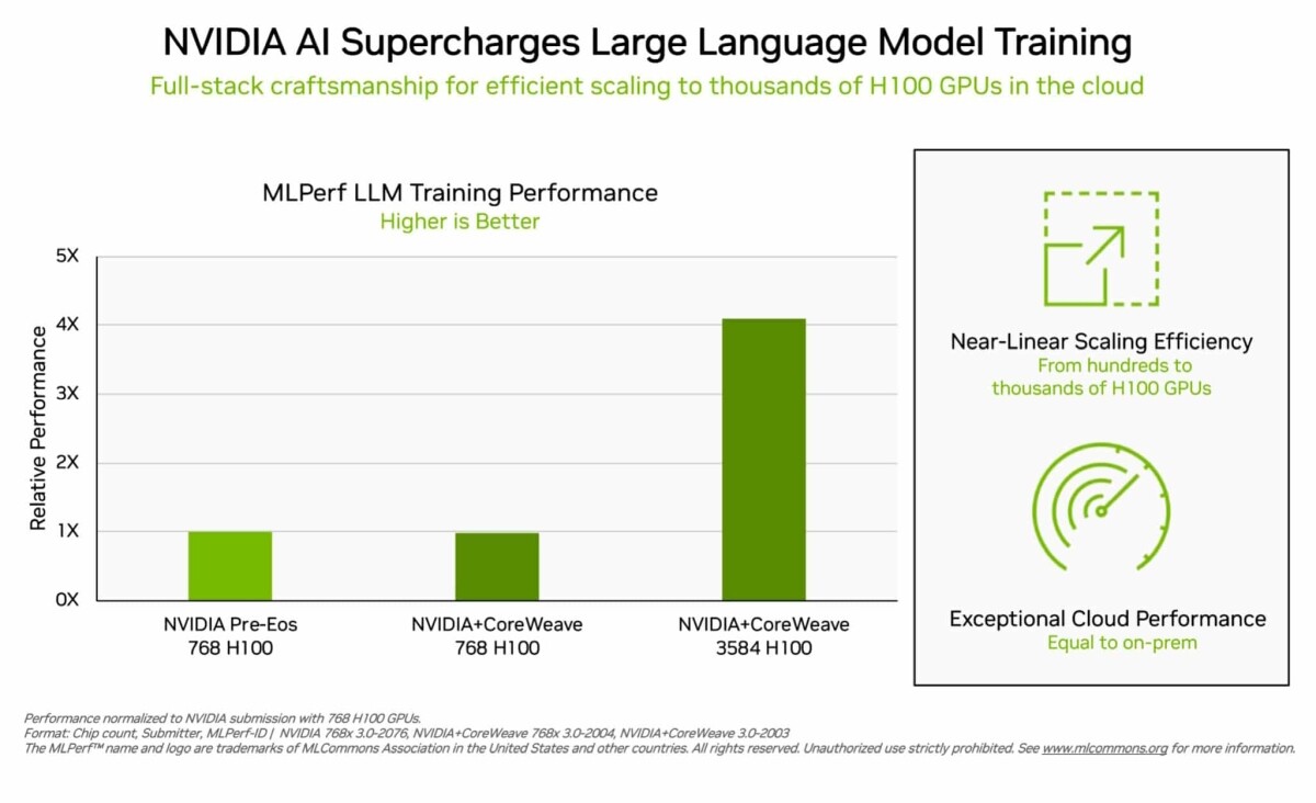
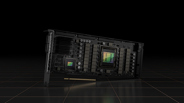
Just announced high-density CPU servers include Intel Xeon-based H263-S63-LAN1 and AMD EPYC-based H273-Z80-LAN1. These 2U 4 node servers employ DLC for all eight CPUs, and although it is dense computing CPU performance achieves its full potential. In August, GIGABYTE announced new servers for NVIDIA HGX H100 GPU, and now adds the DLC version to the G593 series, G593-SD0-LAX1, for NVIDIA HGX H100 8-GPU.
Just announced high-density CPU servers include Intel Xeon-based H263-S63-LAN1 and AMD EPYC-based H273-Z80-LAN1. These 2U 4 node servers employ DLC for all eight CPUs, and although it is dense computing CPU performance achieves its full potential. In August, GIGABYTE announced new servers for NVIDIA HGX H100 GPU, and now adds the DLC version to the G593 series, G593-SD0-LAX1, for NVIDIA HGX H100 8-GPU.