News Posts matching #IP

Return to Keyword Browsing

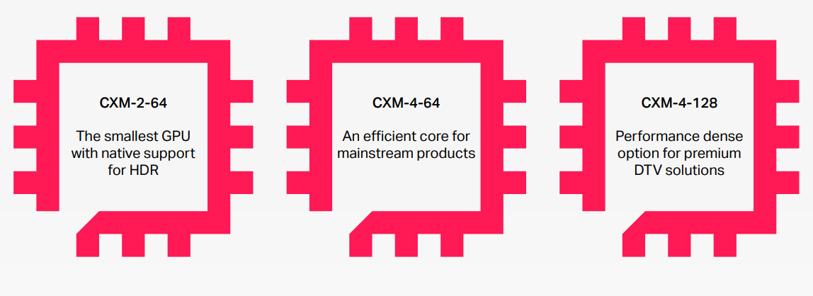
Imagination Technologies Launches the IMG CXM GPU

Imagination Technologies is bringing seamless visual experiences to cost-sensitive consumer devices with the new IMG CXM GPU range which includes the smallest GPU to support HDR user interfaces natively.

Consumers are looking for visuals on their smart home platforms that are as detailed, smooth, and responsive as the experience they are accustomed to on mobile devices. At the same time, ambitious content providers are aligning the look and feel of their applications' user interfaces with their cinematic content, by integrating advanced features such as 4K and HDR.

Ampere Computing Unveils New AmpereOne Processor Family with 192 Custom Cores

Ampere Computing today announced a new AmpereOne Family of processors with up to 192 single threaded Ampere cores - the highest core count in the industry. This is the first product from Ampere based on the company's new custom core, built from the ground up and leveraging the company's internal IP. CEO Renée James, who founded Ampere Computing to offer a modern alternative to the industry with processors designed specifically for both efficiency and performance in the Cloud, said there was a fundamental shift happening that required a new approach.

"Every few decades of compute there has emerged a driving application or use of performance that sets a new bar of what is required of performance," James said. "The current driving uses are AI and connected everything combined with our continued use and desire for streaming media. We cannot continue to use power as a proxy for performance in the data center. At Ampere, we design our products to maximize performance at a sustainable power, so we can continue to drive the future of the industry."

India Homegrown HPC Processor Arrives to Power Nation's Exascale Supercomputer

With more countries creating initiatives to develop homegrown processors capable of powering powerful supercomputing facilities, India has just presented its development milestone with Aum HPC. Thanks to information from the report by The Next Platform, we learn that India has developed a processor for powering its exascale high-performance computing (HPC) system. Called Aum HPC, the CPU was developed by the National Supercomputing Mission of the Indian government, which funded the Indian Institute of Science, the Department of Science and Technology, the Ministry of Electronics and Information Technology, and C-DAC to design and manufacture the Aum HPC processors and create strong, strong technology independence.

The Aum HPC is based on Armv8.4 CPU ISA and represents a chiplet processor. Each compute chiplet features 48 Arm Zeus Cores based on Neoverse V1 IP, so with two chiplets, the processor has 96 cores in total. Each core gets 1 MB of level two cache and 1 MB of system cache, for 96 MB L2 cache and 96 MB system cache in total. For memory, the processor uses 16-channel 32-bit DDR5-5200 with a bandwidth of 332.8 GB/s. To expand on that, HBM memory is present, and there is 64 GB of HBM3 with four controllers capable of achieving a bandwidth of 2.87 TB/s. As far as connectivity, the Aum HPC processor has 64 PCIe Gen 5 Lanes with CXL enabled. It is manufactured on a 5 nm node from TSMC. With a 3.0 GHz typical and 3.5+ GHz turbo frequency, the Aum HPC processor is rated for a TDP of 300 Watts. It is capable of producing 4.6+ TeraFLOPS per socket. Below are illustrations and tables comparing Aum HPC to Fujitsy A64FX, another Arm HPC-focused design.

Bosch Plans to Acquire U.S. Chipmaker TSI Semiconductors

Bosch is expanding its semiconductor business with silicon carbide chips. The technology company plans to acquire assets of the U.S. chipmaker TSI Semiconductors, based in Roseville, California. With a workforce of 250, the company is a foundry for application-specific integrated circuits, or ASICs. Currently, it mainly develops and produces large volumes of chips on 200-millimeter silicon wafers for applications in the mobility, telecommunications, energy, and life sciences industries. Over the next years, Bosch intends to invest more than 1.5 billion USD in the Roseville site and convert the TSI Semiconductors manufacturing facilities to state-of-the-art processes. Starting in 2026, the first chips will be produced on 200-millimeter wafers based on the innovative material silicon carbide (SiC).

In this way, Bosch is systematically reinforcing its semiconductor business, and will have significantly extended its global portfolio of SiC chips by the end of 2030. Above all, the global boom and ramp-up of electromobility are resulting in huge demand for such special semiconductors. The full scope of the planned investment will be heavily dependent on federal funding opportunities available via the CHIPS and Science Act as well as economic development opportunities within the State of California. Bosch and TSI Semiconductors have reached an agreement to not to disclose any financial details of the transaction, which is subject to regulatory approval.

Sega Purchases Angry Birds Game Developer for $776 Million

Today Japan's Sega Sammy Holdings Incorporated declared its intention to fully acquire Finnish development studio Rovio Entertainment Oyj in a buyout valued at a cool $776 million. The Helsinki-based developer, responsible for creating the Angry Birds video game franchise, has agreed to Sega Sammy's terms - and Rovio share values have climbed as a result of this announcement. The deal is expected to be finalized in the late summer or early autumn of this year, and signals an ambition on Sega's part to gain prominence in the mobile gaming world. Rovio had previously turned down a proposed takeover by Playtika - an Israeli company specializing in digital entertainment - for $735 million, late last month.

Angry Birds was the first mobile game to be downloaded one billion times, according to figures released by Rovio, so Sega has acquired a solid intellectual property that has also expanded into the movie world (two animated features) and endless merchandising avenues (toys, clothing and other accessories). Commenting on the buyout, Haruki Satomi, President and Group CEO, Representative Director of Sega Sammy Holdings Inc. said: "Among the rapidly growing global gaming market, the mobile gaming market has especially high potential, and it has been Sega's long-term goal to accelerate its expansion in this field."

Chinese Loongson 3D5000 Features 32 Cores and is 4x Faster Than the Average Arm Chip

Amid the push for technology independence, Chinese companies are pushing out more products to satisfy the need for the rapidly soaring demand for domestic data processing silicon. Today, we have information that Chinese Loongson has launched a 3D5000 CPU with as many as 32 cores. Utilizing chiplet technology, the 3D5000 represents a combination of two 16-core 3C5000 processors based on LA464 cores, based on LoongArch ISA that follows the combination of RISC and MIPS ISA design principles. The new chip features 64 MB of L3 cache, supports eight-channel DDR4-3200 ECC memory achieving 50 GB/s, and has five HyperTransport (HT) 3.0 interfaces. The TDP configuration of the chip is officially 300 Watts; however, normal operation is usually at around 150 Watts, with LA464 cores running at 2 GHz.

Scaling of the new chip goes beyond the chiplet, and pours over into system, as 3D5000 supports 2P and 4P configurations, where a single motherboard can become a system of up to 128 cores. To connect them, Loongson uses a 7A2000 bridge chip that is reportedly 400% faster than the previous solution, although we have no information about the last chip bridge. Based on the LGA-4129 package, the chip size is 75.4x58.5×6.5 mm. Regarding performance, Loongson compares it to the average Arm chip that goes into smartphones and claims that its designs are up to four times faster. In SPEC2006, performance reaches 425 points, while maintaining a single TeraFLOP at dual-precision 64-bit format. On the other hand, the processor was built for security, as the chip has a custom hardware-baked security to prevent Spectre and Meltdown, has an on-package Trusted Platform Module (TPM), and has a secret China-made security algorithm with an embedded custom security module that does encryption and decryption at 5 Gbps.

Rambus and SK hynix Extend Comprehensive License Agreement

Rambus Inc., a premier chip and silicon IP provider making data faster and safer, today announced it has extended its comprehensive patent license agreement with SK hynix, a world leader in advanced semiconductor technology, for an additional ten years. Effective July 1, 2024, the extension maintains similar financial terms and provides SK hynix with broad access to the full Rambus patent portfolio through mid 2034. Other terms and details are confidential.

"SK hynix is a longstanding partner and customer, and we are very pleased to extend our strong relationship well ahead of the agreement's expiration date," said Luc Seraphin, president and chief executive officer of Rambus. "Both Rambus and SK hynix are committed to advancing the industry with world-class products and technology, and this extension is a testament to the ongoing value of our intellectual property and our continued product collaborations together."

UP Team Collaborate with Leopard Imaging to Bring AI Vision to the Edge

Following its successful demonstration of a MIPI camera solution using the UP Squared Pro 7000 at Embedded World, AAEON have announced a MIPI Expansion Kit for the newly released third generation board. Equipped with the Intel Atom Processors x7000E Series, Intel Core i3-N305 Processor and Intel Processor N Series (formerly Alder Lake-N) and an FPC port supporting MIPI-CSI interface, the UP Squared Pro 7000 emphasizes AAEON's continued dedication to bringing the latest Intel technologies to a wider variety of platforms. One such platform is the LI-ADL-ADP-IMX415-MIPI-081H, a 4K MIPI Camera Module from leading intelligent embedded camera creator, Leopard Imaging Inc.

The company recently announced that the camera has been designed with full-function drivers to support the Intel Atom Processors x7000E Series, Intel Core i3-N305 Processor, and Intel Processor N Series (formerly Alder Lake-N), allowing users to take advantage of the peripheral Intel technologies that come with the processor platform, such as Intel UHD Graphics on a Windows 10 IoT Enterprise OS.

Arm to Change Pricing Model Ahead of IPO

Softbank, the owner of Arm Ltd., is preparing everything it can to ensure a successful initial public offering (IPO) of Arm. However, ahead of the IPO, we have more information about Arm's plans to change its licensing and pricing structures to collect more royalties and ensure higher cash flow for future investors. Currently, Arm licenses technology in the form of intellectual property (IP), usually in different flavors of Cortex-A CPU cores that go inside processors for phones and laptops. Chipmakers that use the IP have additional expenses such as Arm ISA license fee and per-chip royalty, which is based on the chip's average selling price.

However, according to Financial Times, we have a new pricing structure that changes how Arm bills its partners and customers. From now on, Arm will grant licenses to chipmakers and ask them to only ship to device makers with an agreement with Arm. Additionally, these device makers now pay per-device royalty based on the device's average selling price (ASP). This ensures that Arm's fee applies to the higher margin product, which means that ultimately Arm will collect more cash flow from its customers and partners. Currently, the old model charges around 1-2 percents per chip in each smartphone, considering the ASP of smartphone chips to be $40 for Qualcomm, $17 for MediaTek, and $6 for Unisoc. However, taking the ASP of a mobile phone at $335, as recorded in 2022, the fee would be much higher. People familiar with the matter noted that Arm will apply this pricing structure as early as 2024. Apple and Samsung are not impacted by this change, as both companies enjoy their own agreements with Arm.

Atari is Acquiring Nightdive Studios

Atari has announced that is buying Nightdive Studios for a cool $10 million - the abandonware specialists will become part of the publisher's larger ambitions to boost production of retro IPs. Nightdive's proprietary KEX engine will form the technological base for future remakes of Atari titles from the archives. As the news of this acquisition hit the web, the Nightdive Twitter posted a positive message regarding the buyout: "This is a big win for our team! As we look to continue producing high-quality, new, and remastered games that do justice to the original IP; we could think of no better long-term partner than."

Nightdive leaders Stephen Kick and Larry Kuperman stated in a joint statement: "Night Dive and Atari have a long history together and we know that Atari shares our passion for retro games and our focus on producing high-quality new and remastered games that do justice to the original IP. As we look to grow our business and expand our capabilities, we could think of no better long-term partner than Atari."

Cadence Announces The First GDDR7 Verification Solution

Cadence, a leading developer of tools for system design and verification, has announced the industry's first GDDR7 verification solution. This in-depth software solution affords IC designers the ability to simulate and verify their GDDR7 silicon designs before printing a single chip. The challenges of designing GDDR7 stem from a rather massive leap in operating speed and advanced features, with GDDR7 targeting speeds of 36,000 MT/s and utilizing more advanced signaling methods.

Biden-Harris Administration Launches First CHIPS for America Funding Opportunity

The Biden-Harris Administration through the U.S. Department of Commerce's National Institute of Standards and Technology today launched the first CHIPS for America funding opportunity for manufacturing incentives to restore U.S. leadership in semiconductor manufacturing, support good-paying jobs across the semiconductor supply chain, and advance U.S. economic and national security.

As part of the bipartisan CHIPS and Science Act, the Department of Commerce is overseeing $50 billion to revitalize the U.S. semiconductor industry, including $39 billion in semiconductor incentives. The first funding opportunity seeks applications for projects to construct, expand, or modernize commercial facilities for the production of leading-edge, current-generation, and mature-node semiconductors. This includes both front-end wafer fabrication and back-end packaging. The Department will also be releasing a funding opportunity for semiconductor materials and equipment facilities in the late spring, and one for research and development facilities in the fall.

Marvell and AWS Collaborate to Enable Cloud-First Silicon Design

Marvell Technology, Inc., a leader in data infrastructure semiconductor solutions, announced today that it has selected Amazon Web Services, Inc. (AWS) as its cloud provider for electronic design automation (EDA). A cloud-first approach helps Marvell to rapidly and securely scale its service on the world's leading cloud, rise to the challenges brought by increasingly complex chip design processes, and deliver continuous innovation for the expanding needs across the automotive, carrier, data center, and enterprise infrastructure markets it serves. The work extends the longstanding relationship between the two companies—Marvell is also a key semiconductor supplier for AWS, helping the company support the design and rapid delivery of cloud services that best meet customers' demanding requirements.

EDA refers to the specialized and compute-intensive processes used in chip making and is a critical piece of Marvell's R&D. Over the years, the number of transistors on an integrated chip has increased exponentially. Each advance in chip design calls for a calculated application of software modules overseeing logic design, debugging, component placement, wire routing, optimization of time and power consumption, and verification. Due to the computationally intensive nature of EDA workloads, it is no longer cost-effective or timely to run EDA on premises. By powering its EDA with AWS, Marvell leverages an unmatched portfolio of services including secure, elastic, high-performance compute capacity in the cloud to solve challenges around speed, latency, security of IP, and data transfer.

Intel Slashes Dividend By Two-Thirds, Updates Capital Allocation

Intel Corporation today announced that its board of directors has reset its dividend policy, reducing the quarterly dividend to $0.125 per share (or $0.50 annually) on the company's common stock. The dividend will be payable on June 1, 2023, to stockholders of record on May 7, 2023. Intel also reaffirmed its first-quarter 2023 business outlook provided at its most recent earnings call, including revenue of between $10.5 billion and $11.5 billion; gross margin of 34.1% on a GAAP basis and 39% on a non-GAAP basis; tax rate of (84%) on a GAAP basis and 13% on a non-GAAP basis; and earnings per share of $(0.80) on a GAAP basis and $(0.15) on a non-GAAP basis.

The decision to decrease the quarterly dividend reflects the board's deliberate approach to capital allocation and is designed to best position the company to create long-term value. The improved financial flexibility will support the critical investments needed to execute Intel's transformation during this period of macroeconomic uncertainty. Since first initiated in 1992, Intel's dividend has delivered more than $80 billion in cash returns to the company's stockholders, and the board is committed to maintaining a competitive dividend.

ASML's Ex-Employee in China Allegedly Stole Confidential Information

The Netherlands-based ASML has reportedly launched a comprehensive investigation into the company's branch in China following reports that one of its former employees allegedly stole confidential information. According to Bloomberg, the employee in question was part of a product life cycle management (PLM) program for ASML's advanced lithography solutions. Specifically, the employee worked for the Teamcenter software division responsible for lithography tool management. This software was used to create digital twins of scanners and other tools and allowed information to be shared among the company's employees. In ASML's case, the software contained all the confidential information about the scanners and how they work, which makes it a target for IP theft. We do not know if this is a China-sponsored action to boost its domestic lithography tool development; however, ASML has issued a statement below.
ASMLWe have experienced unauthorized misappropriation of data relating to proprietary technology by a (now) former employee in China. We promptly initiated a comprehensive internal review. Based upon our initial findings we do not believe that the misappropriation is material to our business. However, as a result of the security incident, certain export control regulations may have been violated. ASML has therefore reported the incident to relevant authorities. We are implementing additional remedial measures in light of this incident.

League of Legends Source Code Stolen in Riot Games Cyberattack

Riot Games provided its first response to last week's cyberattack on its company network. The company alleges that the attackers have exfiltrated with the source-codes for "League of Legends," "Teamfight Tactics," and a proprietary anti-cheat software that's no longer in use. Riot Games assures all that no game user data was compromised with this attack (particularly passwords or payment-instrument details); and at worst the stolen source code could help the attackers create cheats. The company also received a ransom e-mail from the attackers demanding payment, failing which they threaten to release the source code to public; but Riot said that it does not intend to pay. Since user information isn't compromised, and the games themselves are protected by IP laws globally, there's little reason to pay up.

AMD Shows Instinct MI300 Exascale APU with 146 Billion Transistors

During its CES 2023 keynote, AMD announced its latest Instinct MI300 APU, a first of its kind in the data center world. Combining the CPU, GPU, and memory elements into a single package eliminates latency imposed by long travel distances of data from CPU to memory and from CPU to GPU throughout the PCIe connector. In addition to solving some latency issues, less power is needed to move the data and provide greater efficiency. The Instinct MI300 features 24 Zen4 cores with simultaneous multi-threading enabled, CDNA3 GPU IP, and 128 GB of HBM3 memory on a single package. The memory bus is 8192-bit wide, providing unified memory access for CPU and GPU cores. CLX 3.0 is also supported, making cache-coherent interconnecting a reality.

The Instinct MI300 APU package is an engineering marvel of its own, with advanced chiplet techniques used. AMD managed to do 3D stacking and has nine 5 nm logic chiplets that are 3D stacked on top of four 6 nm chiplets with HBM surrounding it. All of this makes the transistor count go up to 146 billion, representing the sheer complexity of a such design. For performance figures, AMD provided a comparison to Instinct MI250X GPU. In raw AI performance, the MI300 features an 8x improvement over MI250X, while the performance-per-watt is "reduced" to a 5x increase. While we do not know what benchmark applications were used, there is a probability that some standard benchmarks like MLPerf were used. For availability, AMD targets the end of 2023, when the "El Capitan" exascale supercomputer will arrive using these Instinct MI300 APU accelerators. Pricing is unknown and will be unveiled to enterprise customers first around launch.

Achronix Announces Speedster7t AC7t1500 FPGA General Availability

In a continuing commitment to enabling industry-leading data acceleration in heterogeneous compute environments, Achronix Semiconductor Corporation, the industry's only independent supplier of high-end FPGAs and eFPGA IP solutions, today announced the production release of its AC7t1500 FPGA and the addition of the power-efficient AC7t800 FPGA to the Achronix Tool Suite.

"The Speedster 7t product family offers unprecedented FPGA-based performance for data acceleration applications," said Steve Mensor, VP of Marketing and Business Development at Achronix. "The release of the AC7t1500 to production along with the addition of the AC7t800 in our ACE design tools gives customers multiple options from this industry-leading, high-performance family that offers FPGA programmability with ASIC-level performance. These advancements give customers confidence that they can design on a robust, validated FPGA product family that meets their high-performance and high-bandwidth needs."

Export Regulations Hinder China's Plans for Custom Arm-Based Processors

The United States has recently imposed several sanctions on technology exports to China. These sanctions are designed to restrict the transfer of specific technologies and sensitive information to Chinese entities, particularly those with ties to the Chinese military or government. The primary motivation behind these sanctions is to protect American national security interests, as well as to protect American companies from unfair competition. According to Financial Times, we have information that Chinese tech Giant, Alibaba, can not access Arm licenses for Neoverse V1 technology. Generally, the technology group where Neoverse V-series falls in is called Wassenaar -- multilateral export control regime (MECR) with 42 participating states. This agreement prohibits the sale of technology that could be used for military purposes.

The US argues that Arm's Neoverse V1 IP is not only a product from UK's Arm but a design made in the US as well, meaning that it is a US technology. Since Alibaba's T-Head group responsible for designing processors that go into Alibaba's cloud services can not use Neoverse V1, it has to look for alternative solutions. The Neoverse V1 and V2 can not be sold in China, while Neoverse N1 and N2 can. Alibaba's T-Head engineer argued, "We feel that the western world sees us as second-class people. They won't sell good products to us even if we have money."

Lattice Extends Low Power Leadership with New Lattice Avant FPGA Platform

Lattice Semiconductor, the low power programmable leader, today unveiled Lattice Avant, a new FPGA platform purpose-built to bring the company's power efficient architecture, small size, and performance leadership to mid-range FPGAs. Lattice Avant offers best-in-class power efficiency, advanced connectivity, and optimized compute that enable Lattice to address an expanded set of customer applications across the Communications, Computing, Industrial, and Automotive markets.

"With Lattice Avant, we extend our low power leadership position in the FPGA industry and are poised to continue our rapid pace of innovation, while also doubling the addressable market for our product portfolio," said Jim Anderson, President and CEO, Lattice Semiconductor. "We created Avant to address our customers' need for compelling mid-range FPGA solutions, and we're excited to help them accelerate their designs with new levels of power efficiency and performance."

Arm Could Change Licensing Model to Charge OEMs Directly

Over the past few weeks, the legal dispute between Arm Ltd. and Qualcomm Inc. has been warming up the eyes of the entire tech community. However, as per the latest court filing, Arm could change its licensing strategy and shift its whole business model into a new direction that would benefit the company directly. Currently, the company provides the intellectual property (IP) that chip makers can use and add to designs mixed with other IPs and custom in-house solutions. That is how the world of electronics design (EDA) works and how many companies operate. However, in the Qualcomm-Arm legal battle, Qualcomm's counterclaim has brought new light about Arm's plans for licensing its hardware designs past 2024.

According to Dylan Patel of SemiAnalysis, who examined court documents, Arm will reportedly change terms to use its IP where the use of other IP mixed with Arm IP is prohibited. If a chip maker plans to use Arm CPU IP, they must also use Arm's GPU/NPU/ISP/DSP IPs. This would result in devices that utilize every design the UK-based designer has to offer, and other IP makers will have to exclude their designs from the SoC. By doing this, Arm directly stands against deals like the Samsung-AMD deal, where AMD provides RDNA GPU IP and would force Samsung to use Arm's Mali GPU IP instead. This change should take effect in 2025 when every new license agreement has to comply with new rules.

Alphawave IP Achieves Its First Testchip Tapeout for TSMC N3E Process

Alphawave IP (LSE: AWE), a global leader in high-speed connectivity for the world's technology infrastructure, today announced the successful tapeout of its ZeusCORE100 1-112 Gbps NRZ/PAM4 Serialiser-Deserialiser ("SerDes"), Alphawave's first testchip on TSMC's most advanced N3E process. Alphawave IP will be exhibiting this new product alongside its complete portfolio of high-performance IP, chiplet, and custom silicon solutions at the TSMC OIP Forum on October 26 in Santa Clara, CA as the Platinum sponsor.

ZeusCORE100 is Alphawave's most advanced multi-standard-SerDes, supporting extra-long channels over 45dB and the most requested standards such as 800G Ethernet, OIF 112G-CEI, PCIe GEN6, and CXL 3.0. Attendees will be able to visit the Alphawave booth and meet the company's technology experts including members of the recently acquired OpenFive team. OpenFive is a longstanding partner of TSMC through the OIP Value Chain Aggregator (VCA) program. OpenFive is one of a select few companies with an idea-to-silicon methodology in TSMC's latest technologies, and advanced packaging capabilities, enabling access to the most advanced foundry solution available with the best Power-Performance-Area (PPA). With Alphawave's industry-leading IP portfolio and the addition of OpenFive's capabilities, designers can create systems on a chip (SoCs) that pack more compute power into smaller form factors for networking, AI, storage, and high-performance computing (HPC) applications.

GIGABYTE Unveils Enterprise-grade Motherboards and an Entry Level Workstation for the Launch of AMD Ryzen 7000 Series

GIGABYTE Technology, (TWSE: 2376), an industry leader in high-performance servers and workstations, today announced supporting products for the new AMD AM5 platform starting with two GIGABYTE motherboards, MC13-LE0 & MC13-LE1, that pair a consumer CPU with IPMI management functionalities via BMC. Additionally, a new desktop workstation, W332-Z00, was released using the same motherboard series platform that supports remote management, but the W332 does so with a Realtek NIC that enables DASH.

The new GIGABYTE products designed to support host systems are deceivingly powerful with a small micro-ATX form factor motherboard and enterprise rich out-of-band management features on top of PCIe Gen 5 and DDR5 technologies. These new client friendly products will be found in office settings under a desk rather than a rack in a data center, as they be managed from anywhere, provided there is a network connection. Furthermore, these new products are purpose built for the mainstream AMD B650E chipset with AMD Zen 4 architecture for AMD Ryzen 7000 Series desktop processors.

Microsoft's Activision-Blizzard Acquisition Hits UK and EU Regulatory Hurdles

Microsoft's USD $68.7 billion acquisition of Activision-Blizzard is running into hurdles with competition regulators in both the UK and the EU, with both Brussels and London hinting at a thorough investigation into the impact the acquisition will have on competition in their respective markets. Microsoft is already a game publisher under Microsoft Games Studio, and makes at least two leading gaming platforms—the Xbox and Windows PC; whereas Activision-Blizzard own a constellation of dozens of game developers, and a mountain of IP over some of the most valuable game franchises of all time.

Britain's Competition and Markets Authority has hinted that the acquisition warrants a "second-phase investigation" since it has concerns that the deal would "result in a substantial lessening of competition within a market or markets in the United Kingdom." Over in Brussels, the EU market regulators, too, are taking a closer look at what the deal could entail for European consumers. Sony Computer Entertainment is particularly unhappy with the acquisition, and is the primary source of opposition to the deal that's invoked by regulators. Sony fears that with this acquisition, Microsoft will be in a position to deny popular game franchises such as "Call of Duty" to the PlayStation platform, and will have too much control over whether Sony can deliver an experience comparable or better than that of the Xbox.
Many Thanks to DeathtoGnomes for the tip.

Report: Apple to Move a Part of its Embedded Cores to RISC-V, Stepping Away from Arm ISA

According to Dylan Patel of SemiAnalysis sources, Apple is moving its embedded cores from Arm to RISC-V. In Apple's Silicon designs, there are far more cores than the main ones that power the operating system and end-user applications. For example, embedded cores are present, and there are 30+ in M1 SoCs responsible for all kinds of workloads not related to the operating system. These tasks are usually associated with other functions such as WiFi/BlueTooth, ThunderBolt retiming, touchpad control, NAND chips having their own core, etc. They run their own firmware and power everything around the central cores that run the OS, so the whole SoC functions appropriately.

It appears that a lot of these cores are based on Arm M-series or lower-end A-series IP that Apple is currently looking to replace with RISC-V. Given that a large portion of software runs on the main big.LITTLE configuration, other secondary SoC tasks can migrate to a different ISA like RISC-V, with a small firmware adjustment. Given that these cores can be placed with custom IPs, Apple would save licensing fees if custom RISC-V cores were used. Additionally, developing firmware for these cores at an Apple engineering team size shouldn't be a problem. Of course, we have no information about when these custom cores will appear inside Apple Silicon. Even when they are used, no formal announcement is expected given that the main cores remain to be powered by Arm ISA, with everything else invisible to the end-user.
Return to Keyword Browsing
Jul 5th, 2025 18:01 CDT change timezone

New Forum Posts

Popular Reviews

TPU on YouTube

Controversial News Posts