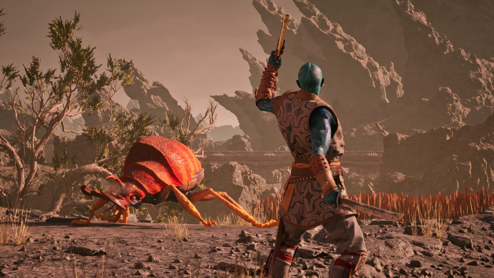
News Posts matching #IP

Return to Keyword Browsing

Alphawave Semi Partners with Keysight to Deliver a Complete PCIe 6.0 Subsystem Solution

Alphawave Semi (LSE: AWE), a global leader in high-speed connectivity for the world's technology infrastructure, today announced successful collaboration with Keysight Technologies, a market-leading design, emulation, and test solutions provider, demonstrating interoperability between Alphawave Semi's PCIe 6.0 64 GT/s Subsystem (PHY and Controller) Device and Keysight PCIe 6.0 64 GT/s Protocol Exerciser, negotiating a link to the maximum PCIe 6.0 data rate. Alphawave Semi, already on the PCI-SIG 5.0 Integrators list, is accelerating next-generation PCIe 6.0 Compliance Testing through this collaboration.

Alphawave Semi's leading-edge silicon implementation of the new PCIe 6.0 64 GT/s Flow Control Unit (FLIT)-based protocol enables higher data rates for hyperscale and data infrastructure applications. Keysight and Alphawave Semi achieved another milestone by successfully establishing a CXL 2.0 link setting the stage for future cache coherency in the datacenter.

MemryX Demos Production Ready AI Accelerator (MX3) During 2024 CES Show

MemryX Inc. is announcing the availability of production level silicon of its cutting-edge AI Accelerator (MX3). MemryX is a pioneering startup specializing in accelerating artificial intelligence (AI) processing for edge devices. In less than 30 days after receiving production silicon from TSMC, MemryX will publicly showcase the ability to efficiently run hundreds of unaltered AI models at the 2024 Consumer Electronics Show (CES) in Las Vegas from Jan 9 through Jan 12.

Chinese Firm Montage Repackages Intel's 5th Generation Emerald Rapids Xeon Processor into Domestic Product Lineup

Chinese chipmaker Montage Technology has unveiled new data center processors under its Jintide brand based on Intel's latest Emerald Rapids Xeon architecture. The 5th generation Jintide lineup offers anywhere from 16-core to 48-core options for enterprise customers needing advanced security specific to China's government and enterprise requirements. Leveraging a long-running joint venture with Intel, Jintide combines standard high-performance Xeon microarchitectures with added on-die monitoring and encryption blocks, PrC (Pre-check) and DSC (Dynamic Security Check), which are security-hardened for sensitive Chinese use cases. The processors retain all core performance attributes of Intel's vanilla offerings thanks to IP access, only with extra protections mandated by national security interests. While missing the very highest core counts, the new Jintide chips otherwise deliver similar Emerald Rapids features like 8-channel DDR5-5600 memory, 80 lanes of speedy PCIe 5.0, and elevated clock speeds over 4.0 GHz at peak. The Jintide processors have 2S scaling, which allows for dual-socket systems with up to 96 cores and 192 threads.

Pricing remains unpublished but likely carries a premium over Intel list prices thanks to the localized security customization required. However, with Jintide uniquely meeting strict Chinese government and data regulations, cost becomes secondary for target customers needing compliant data center hardware. After matching lockstep with Intel's last several leading Xeon generations, Jintide's continued iteration highlights its strategic value in enabling high-performance domestic infrastructure as China eyes IT supply chain autonomy. Intel gets expanded access to the growing Chinese server market, while Chinese partners utilize Intel IP to strengthen localized offerings without foreign dependency. It manifests the delicate balance of advanced chip joint ventures between global tech giants and rising challengers. More details about the SKUs are listed in the table below.

Rapidus and Tenstorrent Partner to Accelerate Development of AI Edge Device Domain Based on 2 nm Logic

Rapidus Corporation, a company involved in the research, development, design, manufacture, and sales of advanced logic semiconductors, today announced an agreement with Tenstorrent Inc., a next-generation computing company building computers for AI, to jointly develop semiconductor IP (design assets) in the field of AI edge devices based on 2 nm logic semiconductors.

In addition to its AI processors and servers, Tenstorrent built and owns the world's most performant RISC-V CPU IP and licenses that technology to its customers around the world. Through this technological partnership with Rapidus, Tenstorrent will accelerate the development of cutting-edge devices to meet the needs of the ever-evolving digital society.

Synopsys Expands Its ARC Processor IP Portfolio with New RISC-V Family

Synopsys, Inc. (Nasdaq: SNPS) today announced it has extended its ARC Processor IP portfolio to include new RISC-V ARC-V Processor IP, enabling customers to choose from a broad range of flexible, extensible processor options that deliver optimal power-performance efficiency for their target applications. Synopsys leveraged decades of processor IP and software development toolkit experience to develop the new ARC-V Processor IP that is built on the proven microarchitecture of Synopsys' existing ARC Processors, with the added benefit of the expanding RISC-V software ecosystem.

Synopsys ARC-V Processor IP includes high-performance, mid-range, and ultra-low power options, as well as functional safety versions, to address a broad range of application workloads. To accelerate software development, the Synopsys ARC-V Processor IP is supported by the robust and proven Synopsys MetaWare Development Toolkit that generates highly efficient code. In addition, the Synopsys.ai full-stack AI-driven EDA suite is co-optimized with ARC-V Processor IP to provide an out-of-the-box development and verification environment that helps boost productivity and quality-of-results for ARC-V-based SoCs.

Ventana Introduces Veyron V2 - World's Highest Performance Data Center-Class RISC-V Processor and Platform

Ventana Micro Systems Inc. today announced the second generation of its Veyron family of RISC-V processors. The new Veyron V2 is the highest performance RISC-V processor available today and is offered in the form of chiplets and IP. Ventana Founder and CEO Balaji Baktha will share the details of Veyron V2 today during his keynote speech at the RISC-V Summit North America 2023 in Santa Clara, California.

"Veyron V2 represents a leap forward in our quest to lead the industry in high-performance RISC-V CPUs that are ready for rapid customer adoption," said Balaji Baktha, Founder and CEO of Ventana. "It substantiates our commitment to customer innovation, workload acceleration, and overall optimization to achieve best in class performance per Watt per dollar. V2 enhancements unleash innovation across data center, automotive, 5G, AI, and client applications."

SiFive to Lay Off Hundreds of Staff Amid Changing RISC-V Market Dynamics

SiFive is a team of one of the pioneering engineers that helped create RISC-V instruction set architecture (ISA) and helped the ecosystem grow. The company has been an active member of the RISC-V community and contributed its guidance on various RISC-V extensions. However, according to sources close to More Than Moore, the company is reportedly downsizing its team, and layoffs are imminent. The impact of the downsizing is about 20% of the workforce, which equals around 120-130 staff. However, that is only part of the story. SiFive is reportedly also canceling its pre-designed core portfolio and shifting focus on custom-design core IP that it would sell to customers. This is in line with the slowing demand for their pre-designed offerings and the growing demand for AI-enhanced custom silicon. The company issued a statement for Moore Than Moore.
SiFive PR for Moore Than MooreAs we adjust to the rapidly changing semiconductor end markets, SiFive is realigning across all of our teams and geographies to better take advantage of the opportunities ahead, reduce operational complexities and increase our ability to respond quickly to customer product requirements. Unfortunately, as a result some positions were eliminated last week. The employees are being offered severance and outplacement assistance. SiFive continues to be excited about the momentum and long-term outlook for our business and RISC-V.
Additionally, there was another statement for More Than Moore, which you can see entirely below.

Arm and Synopsys Strengthen Partnership to Accelerate Custom Silicon on Advanced Nodes

Synopsys today announced it has expanded its collaboration with Arm to provide optimized IP and EDA solutions for the newest Arm technology, including the Arm Neoverse V2 platform and Arm Neoverse Compute Subsystem (CSS). Synopsys has joined Arm Total Design where Synopsys will leverage their deep design expertise, the Synopsys.ai full-stack AI-driven EDA suite, and Synopsys Interface, Security, and Silicon Lifecycle Management IP to help mutual customers speed development of their Arm-based CSS solutions. The expanded partnership builds on three decades of collaboration to enable mutual customers to quickly develop specialized silicon at lower cost, with less risk and faster time to market.

"With Arm Total Design, our aim is to enable rapid innovation on Arm Neoverse CSS and engage critical ecosystem expertise at every stage of SoC development," said Mohamed Awad, senior vice president and general manager, Infrastructure Line of Business at Arm. "Our deep technical collaboration with Synopsys to deliver pre-integrated and validated IP and EDA tools will help our mutual customers address the industry's most complex computing challenges with specialized compute."

Phison Introduces New High-Speed Signal Conditioner IC Products, Expanding its PCIe 5.0 Ecosystem for AI-Era Data Centers

Phison Electronics, a global leader in NAND controllers and storage solutions, announced today that the company has expanded its portfolio of PCIe 5.0 high-speed transmission solutions with PCIe 5.0, CXL 2.0 compatible redriver and retimer data signal conditioning IC products. Leveraging the company's deep expertise in PCIe engineering, Phison is the only signal conditioners provider that offers the widest portfolio of multi-channel PCIe 5.0 redriver and retimer solutions and PCIe 5.0 storage solutions designed specifically to meet the data infrastructure demands of artificial intelligence and machine learning (AI+ML), edge computing, high-performance computing, and other data-intensive, next-gen applications. At the 2023 Open Compute Project Global Summit, the Phison team is showcasing its expansive PCIe 5.0 portfolio, demonstrating the redriver and retimer technologies alongside other enterprise NAND flash, illustrating a holistic vision for a PCIe 5.0 data ecosystem to address the most demanding applications of the AI-everywhere era.

"Phison has focused industry-leading R&D efforts on developing in-house, chip-to-chip communication technologies since the introduction of the PCIe 3.0 protocol, with PCIe 4.0 and PCIe 5.0 solutions now in mass production, and PCIe 6.0 solutions now in the design phase," said Michael Wu, President & General Manager, Phison US. "Phison's accumulated experience in high-speed signaling enables our team to deliver retimer and redriver design solutions that are optimized for top signal integration, low power usage, and high temperature endurance, to deliver interface speeds for the most challenging compute environments."

Tenstorrent Selects Samsung Foundry to Manufacture Next-Generation AI Chiplet

Tenstorrent, a company that sells AI processors and licenses AI and RISC-V IP, announced today that it selected Samsung Foundry to bring Tenstorrent's next generation of AI chiplets to market. Tenstorrent builds powerful RISC-V CPU and AI acceleration chiplets, aiming to push the boundaries of compute in multiple industries such as data center, automotive and robotics. These chiplets are designed to deliver scalable power from milliwatts to megawatts, catering to a wide range of applications from edge devices to data centers.

To ensure the highest quality and cutting-edge manufacturing capabilities for its chiplet, Tenstorrent has selected Samsung's Foundry Design Service team, known for their expertise in silicon manufacturing. The chiplets will be manufactured using Samsung's state-of-the-art SF4X process, which boasts an impressive 4 nm architecture.

Synopsys and TSMC Streamline Multi-Die System Complexity with Unified Exploration-to-Signoff Platform and Proven UCIe IP on TSMC N3E Process

Synopsys, Inc. today announced it is extending its collaboration with TSMC to advance multi-die system designs with a comprehensive solution supporting the latest 3Dblox 2.0 standard and TSMC's 3DFabric technologies. The Synopsys Multi-Die System solution includes 3DIC Compiler, a unified exploration-to-signoff platform that delivers the highest levels of design efficiency for capacity and performance. In addition, Synopsys has achieved first-pass silicon success of its Universal Chiplet Interconnect Express (UCIe) IP on TSMC's leading N3E process for seamless die-to-die connectivity.

"TSMC has been working closely with Synopsys to deliver differentiated solutions that address designers' most complex challenges from early architecture to manufacturing," said Dan Kochpatcharin, head of the Design Infrastructure Management Division at TSMC. "Our long history of collaboration with Synopsys benefits our mutual customers with optimized solutions for performance and power efficiency to help them address multi-die system design requirements for high-performance computing, data center, and automotive applications."

Phanteks Puts Out First Response to Patent Infringement Lawsuit by Lian Li

Phanteks put out its first statement in response to reports about Lian Li filing a patent infringement lawsuit against it. Lian Li alleges that Phanteks D30 RGB line of compound fans for radiators infringe upon a design patent held by the company, and that Lian Li Uni Fan series implement the original design defined in the patent. In particular, the controversy is around the design of the mechanism that lets you daisy-chain individual fans without cables. In its defense, Phanteks says that during the development of the D30 RGB series, its lawyers were duly consulted to look for IP conflicts. The company stated that it will face the legal challenge and is confident to prove that its product is not in infringement of Lian Li IP. The statement by Phanteks follows.
We at Phanteks can confirm the filing of the patent infringement suit filed by a fellow PC enthusiast brand. We want to inform the community that our legal team is and has always properly handled any legal issue or communication that has arose.

From the start of the Phanteks D30 fan development, we set out to design an original product that innovates to provide new solutions to PC enthusiasts. We have consulted with patent lawyers during the development and prior to the announcement of the D30 fans and the fans were not found to infringe on the claims in the patent. Phanteks D30 fans are an original idea and have been issued patents in multiple countries to date.

We value and respect valid and enforceable IP rights and are confident that the result of this legal matter will confirm there is no infringement. We will continue our mission to serve the PC community by creating unique and innovative solutions.

New MIPS CEO Sameer Wasson to Drive Company's RISC-V Market Penetration and Innovation

MIPS, a leading developer of high- performance RISC-V compute IP, has announced embedded systems industry veteran Sameer Wasson as the company's new CEO. Before joining MIPS, Wasson spent 18 years at Texas Instruments (TI), most recently as Vice President, Business Unit (BU) Manager, Processors, where he was responsible for the company's Processor businesses. In that role, Wasson re-established TI as a mainstream microprocessor (MPU) and microcontroller (MCU) supplier for high growth automotive and industrial markets, and established the company's footprint in embedded AI, software defined vehicles, and electrification.

As the new CEO of MIPS, Wasson will further accelerate the company's leadership in the High-Performance RISC-V market as it continues to expand its footprint in Automotive and Enterprise markets.

IT Leaders Optimistic about Ways AI will Transform their Business and are Ramping up Investments

Today, AMD released the findings from a new survey of global IT leaders which found that 3 in 4 IT leaders are optimistic about the potential benefits of AI—from increased employee efficiency to automated cybersecurity solutions—and more than 2 in 3 are increasing investments in AI technologies. However, while AI presents clear opportunities for organizations to become more productive, efficient, and secure, IT leaders expressed uncertainty on their AI adoption timeliness due to their lack of implementation roadmaps and the overall readiness of their existing hardware and technology stack.

AMD commissioned the survey of 2,500 IT leaders across the United States, United Kingdom, Germany, France, and Japan to understand how AI technologies are re-shaping the workplace, how IT leaders are planning their AI technology and related Client hardware roadmaps, and what their biggest challenges are for adoption. Despite some hesitations around security and a perception that training the workforce would be burdensome, it became clear that organizations that have already implemented AI solutions are seeing a positive impact and organizations that delay risk being left behind. Of the organizations prioritizing AI deployments, 90% report already seeing increased workplace efficiency.

Tachyum Achieves 192-Core Chip After Switch to New EDA Tools

Tachyum today announced that new EDA tools, utilized during the physical design phase of the Prodigy Universal Processor, have allowed the company to achieve significantly better results with chip specifications than previously anticipated, after the successful change in physical design tools - including an increase in the number of Prodigy cores to 192.

After RTL design coding, Tachyum began work on completing the physical design (the actual placement of transistors and wires) for Prodigy. After the Prodigy design team had to replace IPs, it also had to replace RTL simulation and physical design tools. Armed with a new set of EDA tools, Tachyum was able to optimize settings and options that increased the number of cores by 50 percent, and SERDES from 64 to 96 on each chip. Die size grew minimally, from 500mm2 to 600mm2 to accommodate improved physical capabilities. While Tachyum could add more of its very efficient cores and still fit into the 858mm2 reticle limit, these cores would be memory bandwidth limited, even with 16 DDR5 controllers running in excess of 7200MT/s. Tachyum cores have much higher performance than any other processor cores.

Intel and Synopsys Expand Partnership to Enable Leading IP on Intel Advanced Process Nodes

Intel and Synopsys announced that they have entered into a definitive agreement to expand the companies' long-standing IP (intellectual property) and EDA (electronic design automation) strategic partnership with the development of a portfolio of IP on Intel 3 and Intel 18A for Intel's foundry customers. The availability of key IP on Intel advanced process nodes will create a more robust offering for new and existing Intel Foundry Services (IFS) customers.

"Marking another important step in our IDM 2.0 strategy, this transaction will foster a vibrant foundry ecosystem by allowing designers to fully realize the advantages of Intel 3 and Intel 18A process technologies and quickly bring differentiated products to market," said Stuart Pann, senior vice president and general manager of IFS. "Synopsys brings a strong track record of delivering high-quality IP to a broad customer base, and this agreement will help accelerate the availability of IP on advanced IFS nodes for mutual customers."

Cadence to Acquire Rambus PHY IP Assets

Cadence Design Systems, Inc. and Rambus Inc., a premier chip and silicon IP provider making data faster and safer, today announced that they have entered into a definitive agreement for Cadence to acquire the Rambus SerDes and memory interface PHY IP business. Rambus will retain its digital IP business, including memory and interface controllers and security IP. The expected technology asset purchase also brings Cadence proven and experienced PHY engineering teams in the United States, India and Canada, further expanding Cadence's domain-rich talent base.

"Memory and SerDes IP design and integration continues to be integral to the design of AI, data center and hyperscale applications, CPU architectures and networking devices, and the addition of the Rambus IP and seasoned team further accelerates Cadence's Intelligent System Design strategy, which drives design excellence," said Boyd Phelps, senior vice president and general manager of the IP Group at Cadence. "The acquisition of the Rambus PHY IP broadens Cadence's well-established enterprise IP portfolio and expands its reach across geographies and vertical markets, such as the aerospace and defense market, providing complete subsystem solutions that meet the demands of our worldwide customers."

Intel Expects to Beat TSMC at 2nm, Intel Foundry to Operate Almost as a Separate Business

Intel's integrated device manufacturing (IDM) has been experiencing a lot of trouble in recent years, and the company is not a leading-edge semiconductor manufacturer, with TSMC taking the pole position. However, the new restructuring hopes to change some of the business operations to increase its efficiency and establish Intel as the go-to foundry for customers. David Zinsner, Executive Vice President and the Chief Financial Officer, alongside Jason Grebe, Corporate Vice President & GM of the Corporate Planning Group at Intel, joined investors to explain how IDM will transform into a next-generation business. Intel IDM, including Intel Foundry Services (IFS), will get a new operation model, which will put IDM as an almost separate business unit with its own profit and loss (P&L) statement published in the quarterly/yearly financial report.

According to Intel, the company's IDM 1.0 strategy has been serving it well, but IDM 2.0 is needed to build next-generation nodes as the capital required for them is massive. Intel hopes to regain node leadership with the Intel 18A node in 2025. The company's strategy is still to have IFS as the second biggest external foundry business, presumably just behind TSMC. Putting IDM into its own P&L will result in $8-10 billion in "cost reduction opportunities, " including ramp rates, test time, and sort times based on the market pricing, not Intel's pricing. At the start, IDM is expected o start with a negative operating margin. Intel also states that keeping IFS as a business unit allows the company to simultaneously develop products on it and de-risk it for customers who want to build on IFS. The company is developing five different products (assuming packaging) on Intel 18A, all of which will be available for customers to use as well.

ITRI Set to Strengthen Taiwan-UK Collaboration on Semiconductors

The newly established Department for Science, Innovation and Technology (DSIT) in the UK has recently released the UK's National Semiconductor Strategy. Dr. Shih-Chieh Chang, General Director of Electronic and Optoelectronic System Research Laboratories at the Industrial Technology Research Institute (ITRI) of Taiwan had an initial exchange with DSIT. During the exchange, Dr. Chang suggested that Taiwan can become a trustable partner for the UK and that the partnership can leverage collective strengths to create mutually beneficial developments. According to the Strategy, the British government plans to invest 1 billion pounds over the next decade to support the semiconductor industry. This funding will improve access to infrastructure, power more research and development and facilitate greater international cooperation.

Dr. Chang stressed that ITRI looks forward to more collaboration with the UK on semiconductors to enhance the resilience of the supply chain. While the UK possesses cutting-edge capabilities in semiconductor IP design and compound semiconductor technology, ITRI has extensive expertise in semiconductor technology R&D and trial production. As a result, ITRI is well-positioned to offer consultation services for advanced packaging pilot lines, facilitate pre-production evaluation, and link British semiconductor IP design companies with Taiwan's semiconductor industry chain. "The expansion of British manufacturers' service capacity in Taiwan would create a mutually beneficial outcome for both Taiwan and the UK," said Dr. Chang.

Realtek Takes MediaTek to Court Over Third Party Patent Dispute

A legal dispute between Realtek and MediaTek has kicked off over Realtek claiming that MediaTek has gotten a third party company to sue Realtek over some unspecified patents involving technology used in smart TVs and set-top boxes. The third party involved goes under the name of IPValue Management Inc and appears to be what is generally known as a patent troll, i.e. a company that buys up patents and uses them to take legal actions against other companies, without actually producing anything related to the patents in question. Realtek claims that MediaTek is conspiring with IPValue to drive Realtek out of the market, leaving Mediatek in a close to monopoly situation in the market.

According to Reuters, Realtek told the publication that it filed the lawsuit against MediaTek to "protect free and fair competition in the industry" and "prevent further harm to the public." Neither MediaTek or IPValue have commented on the lawsuit to the publication. What makes this entire mess even more peculiar, is that MediaTek is said to have a licensing agreement in place with a subsidiary of IPValue called Future Link System LLC, which was signed in 2019. This agreement was brought up by the U.S. International Trade Commission (ITC) in a separate lawsuit last year, with the ITC calling it alarming and the court calling it improper. After the ITC criticism last year, Future Link apparently settled with several other companies such as Amlogic, but not with Realtek, which is why the company is now taking things to court. Realtek claims that MediaTek is trying to force any allegedly infringing chips out of the market and trying to make Realtek look like an unreliable partner and supplier to its customers. As such, Realtek wants the court to end the alleged conspiracy and is also asking for damages. Time will tell if Realtek is successful or not, but it seems strange that a patent troll would agree to licence its patents to some parties, but not all, since the only reason for a patent troll to exist is to make money from its patents.

Intel Falcon Shores is Initially a GPU, Gaudi Accelerators to Disappear

During the ISC High Performance 2023 international conference, Intel announced interesting roadmap updates to its high-performance computing (HPC) and artificial intelligence (AI). With the scrapping of Rialto Bridge and Lancaster Sound, Intel merged these accelerator lines into Falcon Shores processor for HPC and AI, initially claiming to be a CPU+GPU solution on a single package. However, during the ISC 2023 talk, the company forced a change of plans, and now, Falcon Shores is GPU only solution destined for a 2025 launch. Originally, Intel wanted to combine x86-64 cores with Xe GPU to form an "XPU" module that powers HPC and AI workloads. However, Intel did not see a point in forcing customers to choose between specific CPU-to-GPU core ratios that would need to be in an XPU accelerator. Instead, a regular GPU solution paired with a separate CPU is the choice of Intel for now. In the future, as workloads get more defined, XPU solutions are still a possibility, just delayed from what was originally intended.

Regarding Intel's Gaudi accelerators, the story is about to end. The company originally paid two billion US Dollars for Habana Labs and its Gaudi hardware. However, Intel now plans to stop the Gaudi development as a standalone accelerator and instead use the IP to integrate it into its Falcon Shores GPU. Using modular, tile-based architecture, the Falcon Shores GPU features standard ethernet switching, up to 288 GB of HBM3 running at 9.8 TB/s throughput, I/O optimized for scaling, and support for FP8 and FP16 floating point precision needed for AI and other workloads. As noted, the creation of XPU was premature, and now, the initial Falcon Shores GPU will become an accelerator for HPC, AI, and a mix of both, depending on a specific application. You can see the roadmap below for more information.

Imagination Technologies Launches the IMG CXM GPU

Imagination Technologies is bringing seamless visual experiences to cost-sensitive consumer devices with the new IMG CXM GPU range which includes the smallest GPU to support HDR user interfaces natively.

Consumers are looking for visuals on their smart home platforms that are as detailed, smooth, and responsive as the experience they are accustomed to on mobile devices. At the same time, ambitious content providers are aligning the look and feel of their applications' user interfaces with their cinematic content, by integrating advanced features such as 4K and HDR.

Ampere Computing Unveils New AmpereOne Processor Family with 192 Custom Cores

Ampere Computing today announced a new AmpereOne Family of processors with up to 192 single threaded Ampere cores - the highest core count in the industry. This is the first product from Ampere based on the company's new custom core, built from the ground up and leveraging the company's internal IP. CEO Renée James, who founded Ampere Computing to offer a modern alternative to the industry with processors designed specifically for both efficiency and performance in the Cloud, said there was a fundamental shift happening that required a new approach.

"Every few decades of compute there has emerged a driving application or use of performance that sets a new bar of what is required of performance," James said. "The current driving uses are AI and connected everything combined with our continued use and desire for streaming media. We cannot continue to use power as a proxy for performance in the data center. At Ampere, we design our products to maximize performance at a sustainable power, so we can continue to drive the future of the industry."

India Homegrown HPC Processor Arrives to Power Nation's Exascale Supercomputer

With more countries creating initiatives to develop homegrown processors capable of powering powerful supercomputing facilities, India has just presented its development milestone with Aum HPC. Thanks to information from the report by The Next Platform, we learn that India has developed a processor for powering its exascale high-performance computing (HPC) system. Called Aum HPC, the CPU was developed by the National Supercomputing Mission of the Indian government, which funded the Indian Institute of Science, the Department of Science and Technology, the Ministry of Electronics and Information Technology, and C-DAC to design and manufacture the Aum HPC processors and create strong, strong technology independence.

The Aum HPC is based on Armv8.4 CPU ISA and represents a chiplet processor. Each compute chiplet features 48 Arm Zeus Cores based on Neoverse V1 IP, so with two chiplets, the processor has 96 cores in total. Each core gets 1 MB of level two cache and 1 MB of system cache, for 96 MB L2 cache and 96 MB system cache in total. For memory, the processor uses 16-channel 32-bit DDR5-5200 with a bandwidth of 332.8 GB/s. To expand on that, HBM memory is present, and there is 64 GB of HBM3 with four controllers capable of achieving a bandwidth of 2.87 TB/s. As far as connectivity, the Aum HPC processor has 64 PCIe Gen 5 Lanes with CXL enabled. It is manufactured on a 5 nm node from TSMC. With a 3.0 GHz typical and 3.5+ GHz turbo frequency, the Aum HPC processor is rated for a TDP of 300 Watts. It is capable of producing 4.6+ TeraFLOPS per socket. Below are illustrations and tables comparing Aum HPC to Fujitsy A64FX, another Arm HPC-focused design.

Bosch Plans to Acquire U.S. Chipmaker TSI Semiconductors

Bosch is expanding its semiconductor business with silicon carbide chips. The technology company plans to acquire assets of the U.S. chipmaker TSI Semiconductors, based in Roseville, California. With a workforce of 250, the company is a foundry for application-specific integrated circuits, or ASICs. Currently, it mainly develops and produces large volumes of chips on 200-millimeter silicon wafers for applications in the mobility, telecommunications, energy, and life sciences industries. Over the next years, Bosch intends to invest more than 1.5 billion USD in the Roseville site and convert the TSI Semiconductors manufacturing facilities to state-of-the-art processes. Starting in 2026, the first chips will be produced on 200-millimeter wafers based on the innovative material silicon carbide (SiC).

In this way, Bosch is systematically reinforcing its semiconductor business, and will have significantly extended its global portfolio of SiC chips by the end of 2030. Above all, the global boom and ramp-up of electromobility are resulting in huge demand for such special semiconductors. The full scope of the planned investment will be heavily dependent on federal funding opportunities available via the CHIPS and Science Act as well as economic development opportunities within the State of California. Bosch and TSI Semiconductors have reached an agreement to not to disclose any financial details of the transaction, which is subject to regulatory approval.
Return to Keyword Browsing
Aug 14th, 2024 14:08 EDT change timezone

New Forum Posts

Popular Reviews

Controversial News Posts