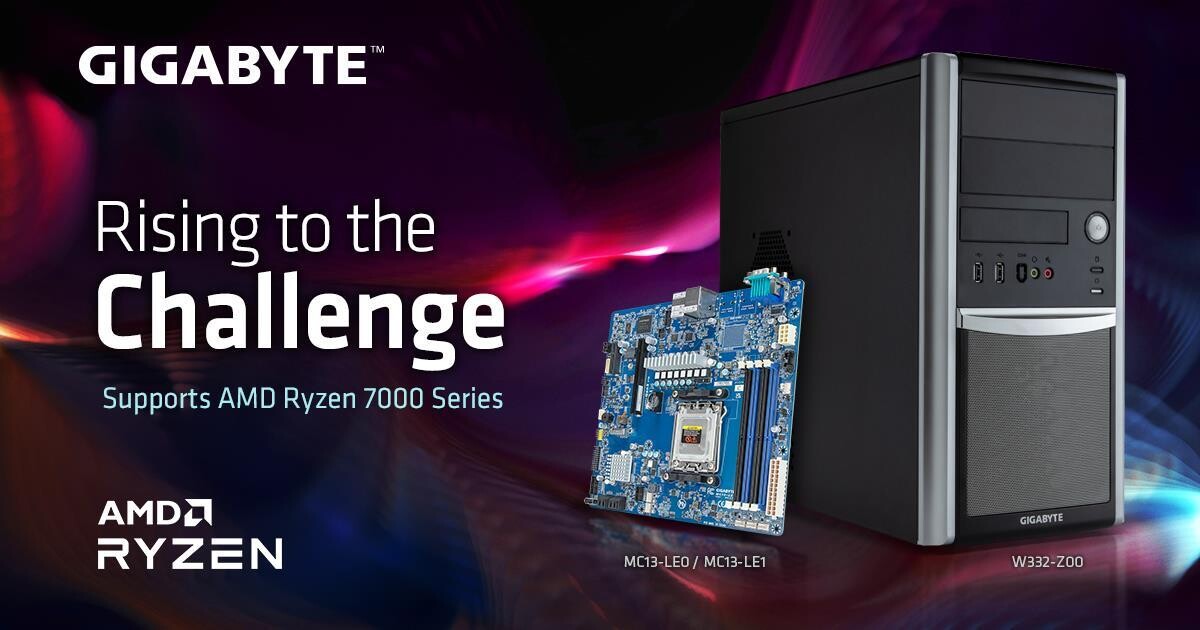
News Posts matching #IP

Return to Keyword Browsing

Tachyum Prodigy Software Emulation Systems Now Available for Pre-Order

Tachyum Inc. today announced that it is signing early adopter customers for the software emulation system for its Prodigy Universal Processor, customers may begin the process of native software development (i.e. using Prodigy Instruction Set Architecture) and porting applications to run on Prodigy. Prodigy software emulation systems will be available at the end of January 2021.

Customers and partners can use Prodigy's software emulation for evaluation, development and debug, and with it, they can begin to transition existing applications that demand high performance and low power to run optimally on Prodigy processors. Pre-built systems include a Prodigy emulator, native Linux, toolchains, compilers, user mode applications, x86, ARM and RISC-V emulators. Software updates will be issued as needed.

QNAP Launches the QGD-3014-16PT Desktop Smart Edge PoE Switch

QNAP Systems, Inc., a leading computing, networking and storage solution innovator, today announced the desktop smart edge PoE Switch - QGD-3014-16PT. With sixteen 30-watt Gigabit PoE ports, two 2.5GbE host management ports, Intel Celeron J4125 quad-core 2.0 GHz processor, and four 3.5-inch SATA drive bays, the QGD-3014-16PT supports QVR Pro, HBS 3 and QuWAN SD-WAN to integrate surveillance deployment, video storage computing, and multi-site remote management to offer SMBs innovative intelligent IP surveillance infrastructure and remote backup solutions.
"Expanding multi-site surveillance networks can be costly and involve large amounts of equipment with low transmission efficiency between multiple remote devices - not to mention the complexities involved in deployment and management. " said Daniel Hsieh, QNAP Product Manager, adding, "the QGD-3014-16PT desktop Smart Edge PoE Switch integrates PoE, surveillance capabilities, and data backup management to simplify these requirements and increase the transmission and backup efficiency of surveillance videos."

AWS and Arm Demonstrate Production-Scale Electronic Design Automation in the Cloud

Today, Amazon Web Services, Inc. (AWS), an Amazon.com, Inc. company, announced that Arm, a global leader in semiconductor design and silicon intellectual property development and licensing, will leverage AWS for its cloud use, including the vast majority of its electronic design automation (EDA) workloads. Arm is migrating EDA workloads to AWS, leveraging AWS Graviton2-based instances (powered by Arm Neoverse cores), and leading the way for transformation of the semiconductor industry, which has traditionally used on-premises data centers for the computationally intensive work of verifying semiconductor designs.

To carry out verification more efficiently, Arm uses the cloud to run simulations of real-world compute scenarios, taking advantage of AWS's virtually unlimited storage and high-performance computing infrastructure to scale the number of simulations it can run in parallel. Since beginning its AWS cloud migration, Arm has realized a 6x improvement in performance time for EDA workflows on AWS. In addition, by running telemetry (the collection and integration of data from remote sources) and analysis on AWS, Arm is generating more powerful engineering, business, and operational insights that help increase workflow efficiency and optimize costs and resources across the company. Arm ultimately plans to reduce its global datacenter footprint by at least 45% and its on-premises compute by 80% as it completes its migration to AWS.

RISC-V Processor Achieves 5 GHz Frequency at Just 1 Watt of Power

Researchers at the University of California, Berkeley in 2010 have started an interesting project. They created a goal to develop a new RISC-like Instruction Set Architecture that is simple and efficient while being open-source and royalty-free. Born out of that research was RISC-V ISA, the fifth iteration of Reduced Instruction Set Computing (RISC) ideology. Over the years, the RISC-V ISA has become more common, and today, many companies are using it to design their processors and release new designs every day. One of those companies is Micro Magic Inc., a provider of silicon design tools, IP, and design services. The company has developed a RISC-V processor that is rather interesting.

Apart from the RISC-V ISA, the processor has an interesting feature. It runs at the whopping 5 GHz frequency, a clock speed unseen on the RISC-V chips before, at the power consumption of a mere one (yes that is 1) Watt. The chip ran at just 1.1 Volts, which means that a very low current needs to be supplied to the chip so it can achieve the 5 GHz mark. If you are wondering about performance, well the numbers show that at 5 GHz, the CPU can produce a score of 13000 CoreMarks. However, that is not the company's highest-performance RISC-V core. In yesterday's PR, Micro Magic published that their top-end design can achieve 110000 CoreMarks/Watt, so we are waiting to hear more details about it.

Samsung's 5 nm Node in Production, First SoCs to Arrive Soon

During its Q3 earnings call, Samsung Electronics has provided everyone with an update on its foundry and node production development. In the past year or so, Samsung's foundry has been a producer of a 7 nm LPP (Low Power Performance) node as its smallest node. That is now changed as Samsung has started the production of the 5 nm LPE (Low Power Early) semiconductor manufacturing node. In the past, we have reported that the company struggled with yields of its 5 nm process, however, that seems to be ironed out and now the node is in full production. To contribute to the statement that the new node is doing well, we also recently reported that Samsung will be the sole manufacturer of Qualcomm Snapdragon 875 5G SoC.

The new 5 nm semiconductor node is a marginal improvement over the past 7 nm node. It features a 10% performance improvement that is taking the same power and chip complexity or a 20% power reduction of the same processor clocks and design. When it comes to density, the company advertises the node with x1.33 times increase in transistor density compared to the previous node. The 5LPE node is manufactured using the Extreme Ultra-Violet (EUV) methodology and its FinFET transistors feature new characteristics like Smart Difusion Break isolation, flexible contact placement, and single-fin devices for low power applications. The node is design-rule compatible with the previous 7 nm LPP node, so the existing IP can be used and manufactured on this new process. That means that this is not a brand new process but rather an enhancement. First products are set to arrive with the next generation of smartphone SoCs, like the aforementioned Qualcomm Snapdragon 875.

IP Theft: UMC Pleads Guilty to US Court Charges of Trade Secret Theft, Faces $60 Million Fine

Taiwanese corporation United Micro Electronics (UMC) has pled guilty on charges of trade theft. The charges, originally pressed in November 2018 by US authorities, placed UMC and China's Fujian Jinhua in hot waters under suspicion of stealing trade secrets from US-based Micron technologies, one of the world's foremost players in memory semiconductor technologies. UMC's guilty plea serves as a way for the company to avoid heavier penalties, and includes a provision for the company's assistance in investigating Fujian Jinhua's actions in regards to this IP theft.

The whole story revolves around UMC's hiring of three Micron employees from Micron's subsidiary in Taiwan, Micron Memory Taiwan (MMT), back around September 2015. At least two of these employees migrated Micron trade secrets to UMC, which then inked a deal with china's Fujian Jinhua for the development of 32nm DRAM and "32Snm" DRAM technologies that Fujian Jinhua could then deploy for the manufacture of memory products - a deal which had Fujian Jinhua paying $300 million for equipment purchase plus $400 million for technology development to UMC. This all fell in line with the Chinese government's Made in China 2025 plan, which aims to bring the country to semiconductor independence from the western world. UMC says that the company itself didn't partake in the underhanded IP delivery to Fujian Jinhua, claiming instead that rogue employees did so of their own volition. The company further states that it only pleads guilty because according to the US Trade Secrets Act, the company still bears legal responsibilities for employee acts, whether or not top management is involved.

Intel Confirms Rocket Lake-S Features Cypress Cove with Double-Digit IPC Increase

Today, Intel has decided to surprise us and give an update to its upcoming CPU lineup for desktop. With the 11th generation, Core CPUs codenamed Rocket Lake-S, Intel is preparing to launch the new lineup in the first quarter of 2021. This means that we are just a few months away from this launch. When it comes to the architecture of these new processors, they are going to be based on a special Cypress Cove design. Gone are the days of Skylake-based designs that were present from the 6th to 10th generation processors. The Cypress Cove, as Intel calls it, is an Ice Lake adaptation. Contrary to the previous rumors, it is not an adaptation of Tiger Lake Willow Cove, but rather Ice Lake Sunny Cove.

The CPU instruction per cycle (IPC) is said to grow in double-digits, meaning that the desktop users are finally going to see an improvement that is not only frequency-based. While we do not know the numbers yet, we can expect them to be better than the current 10th gen parts. For the first time on the Intel platform for desktops, we will see the adoption of PCIe 4.0 chipset, which will allow for much faster SSD speeds and support the latest GPUs, specifically, there will be 20 PCIe 4.0 lanes coming from the CPU only. The CPU will be paired with 12th generation Xe graphics, like the one found in Tiger Lake CPUs. Other technologies such as Deep Learning Boost and VNNI, Quick Sync Video, and better overclocking tuning will be present as well. Interesting thing to note here is that the 10C/20T Core i9-10900K has a PL1 headroom of 125 W, and 250 W in PL2. However, the 8C/16T Rocket Lake-S CPU also features 125 W headroom in PL1, and 250 W in PL2. This indicates that the new Cypress Cove design runs hotter than the previous generation.

Apple A14 SoC Put Under the Microscope; Die Size, and Transistor Density Calculated

Apple has established itself as a master of silicon integrated circuit design and has proven over the years that its processors deliver the best results, generation after generation. If we take a look at the performance numbers of the latest A14 Bionic, you can conclude that its performance is now rivaling some of the x86_64 chips. So you would wonder, what is inside this SoC that makes it so fast? That is exactly what ICmasters, a semiconductor reverse engineering and IP services company, has questioned and decided to find out. For starters, we know that Apple manufactures the new SoCs on TSMC's N5 5 nm node. The Taiwanese company promises to pack 171.3 million transistors per square millimeter, so how does it compare to an actual product?

ICmasters have used electron microscopy to see what the chip is made out of and to measure the transistor density. According to this source, Apple has a chip with a die size of 88 mm², which packs 11.8 billion N5 transistors. The density metric, however, doesn't correspond to that of TSMC. Instead of 171.3 million transistors per mm², the ICmasters measured 134.09 million transistors per mm². This is quite a difference, however, it is worth noting that each design will have it different due to different logic and cache layout.
Apple A14 SoC Die Apple A14 SoC

AMD Ryzen 5 5600X Takes the Crown of the Fastest CPU in Passmark Single-Thread Results

AMD has been improving its Zen core design, and with the latest Zen 3 IP found in Ryzen 5000 series CPUs, it seems like the company struck gold. Thanks to the reporting of VideoCardz, we come to know that AMD's upcoming Ryzen 5 5600X CPU has been benchmarked and compared to other competing offerings. In the CPU benchmark called PassMark, which rates all of the CPUs by multi-threaded and single-threaded performance, AMD's Ryzen 5 5600X CPU has taken the crown of the fastest CPU in the single-threaded results chart. Scoring an amazing 3495 points, it is now the fastest CPU for 1T workloads. That puts the CPU above Intel's current best—Core i9-10900K—which scores 3177 points. This puts the Zen 3 core about 10% ahead of the competition.

As a reminder, the AMD Ryzen 5 5600X CPU is a six-core, twelve threaded design that has a base clock of 3.7 GHz and boosts the frequency of the cores to 4.6 GHz, all within the TDP of 65 Watts. The CPU has 32 MB of level-3 (L3) cache and 3 MB of L2 cache.

Dialog Semiconductor Licenses its Non-Volatile ReRAM Technology to GLOBALFOUNDRIES for 22FDX Platform

DIALOG SEMICONDUCTOR, a leading provider of battery and power management, Wi-Fi and Bluetooth low energy (BLE) and Industrial edge computing solutions and GLOBALFOUNDRIES (GF ), the world's leading specialty foundry, today announced that they have entered into an agreement in which Dialog licenses its Conductive Bridging RAM (CBRAM) technology to GLOBALFOUNDRIES. The resistive ram (ReRAM)-based technology was pioneered by Adesto Technologies which was recently acquired by Dialog Semiconductor in 2020. GLOBALFOUNDRIES will first offer Dialog's CBRAM as an embedded, non-volatile memory (NVM) option on its 22FDX platform, with the plan to extend to other platforms.

Dialog's proprietary and production proven CBRAM technology is a low power NVM solution designed to enable a range of applications from IoT and 5G connectivity to artificial intelligence (AI). Low power consumption, high read/write speeds, reduced manufacturing costs and tolerance for harsh environments make CBRAM particularly suitable for consumer, medical, and select industrial and automotive applications. Furthermore, CBRAM technology enables cost-effective embedded NVM for advanced technology nodes required for products in these markets.

Intel Introduces new Security Technologies for 3rd Generation Intel Xeon Scalable Platform, Code-named "Ice Lake"

Intel today unveiled the suite of new security features for the upcoming 3rd generation Intel Xeon Scalable platform, code-named "Ice Lake." Intel is doubling down on its Security First Pledge, bringing its pioneering and proven Intel Software Guard Extension (Intel SGX) to the full spectrum of Ice Lake platforms, along with new features that include Intel Total Memory Encryption (Intel TME), Intel Platform Firmware Resilience (Intel PFR) and new cryptographic accelerators to strengthen the platform and improve the overall confidentiality and integrity of data.

Data is a critical asset both in terms of the business value it may yield and the personal information that must be protected, so cybersecurity is a top concern. The security features in Ice Lake enable Intel's customers to develop solutions that help improve their security posture and reduce risks related to privacy and compliance, such as regulated data in financial services and healthcare.

Imagination Launches IMG B-Series: Doing More with Multi-Core, up to 6 TeraFLOPs of Compute

Imagination Technologies announces IMG B-Series, a new expanded range of GPU IP. With its advanced multi-core architecture, B-Series enables Imagination customers to reduce power while reaching higher levels of performance than any other GPU IP on the market. It delivers up to 6 TFLOPS of compute, with an up to 30% reduction in power and 25% area reduction over previous generations and up to 2.5x higher fill rate than competing IP cores.

With IMG A-Series Imagination made an exceptional leap over previous generations, resulting in an industry-leading position for performance and power characteristics. B-Series is a further evolution delivering the highest performance per mm² for GPU IP and offering new configurations for lower power and up to 35% lower bandwidth for a given performance target, making it a compelling solution for top-tier designs.

Arm Highlights its Next Two Generations of CPUs, codenamed Matterhorn and Makalu, with up to a 30% Performance Uplift

Editor's Note: This is written by Arm vice president and general manager Paul Williamson.

Over the last year, I have been inspired by the innovators who are dreaming up solutions to improve and enrich our daily lives. Tomorrow's mobile applications will be even more imaginative, immersive, and intelligent. To that point, the industry has come such a long way in making this happen. Take app stores for instance - we had the choice of roughly 500 apps when smartphones first began shipping in volume in 2007 and today there are 8.9 million apps available to choose from.

Mobile has transformed from a simple utility to the most powerful, pervasive device we engage with daily, much like Arm-based chips have progressed to more powerful but still energy-efficient SoCs. Although the chip-level innovation has already evolved significantly, more is still required as use cases become more complex, with more AI and ML workloads being processed locally on our devices.

Intel 10 nm Ice Lake-SP Server Processors Reportedly Delayed

Intel 10 nm products have seen massive delays over the years, and Intel has built many IPs on the new node, however, not many of them have seen the light of the day due to problems the company has experienced with the manufacturing of the new node. That has caused delays in product shipments in the past, meaning that the time for 10 nm is just ahead. According to the latest DigiTimes Taiwan report, we have information that Intel is going to delay its Ice Lake-SP server processors manufactured on a 10 nm node. And it is going to be a whole quarter late according to the report. Instead of launching in Q4 this year, we can expect to see new processors in Q1 of 2021. It is yet unknown whatever the launch will happen at the beginning of Q1 or its end, however, we will report on it as we hear more information.

Update: DigiTimes has also released another report regarding server shipments. It is reported that server vendors are decelerating the shipments as they are making fewer orders in Q4 to wait for the new Intel CPUs. Judging by this move, the demand for these new processors is going to be rather high and the supply chain is preparing slowly for it.

Arm Spins-out Cerfe Labs to Advance Development of CeRAM Memory Technology

Today Arm announced the spin-out of Cerfe Labs to develop and license new types of non-volatile memories based on correlated electron materials (CeRAM) and ferroelectric transistors (FeFETs). Arm CeRAM researchers will join Cerfe Labs and assume ownership of the Arm joint development project with Symetrix Corporation.

As part of the spin-out, Arm will transfer its full CeRAM IP portfolio of more than 150 patent families to Cerfe Labs that will be the foundation for a roadmap of related CeRAM technologies. Cerfe Labs initial focus will be on producing meaningful prototypes which will be licensed to partners with a goal of accelerating timing of enabling these novel non-volatile materials for systems.

New Arm Technologies Enable Safety-capable Computing Solutions for an Autonomous Future

Today, Arm unveiled new computing solutions to accelerate autonomous decision-making with safety capability across automotive and industrial applications. The new suite of IP includes the Arm Cortex -A78AE CPU, Arm Mali -G78AE GPU, and Arm Mali-C71AE ISP, engineered to work together in combination with supporting software, tools and system IP to enable silicon providers and OEMs to design for autonomous workloads. These products will be deployed in a range of applications, from enabling more intelligence and configurability in smart manufacturing to enhancing ADAS and digital cockpit applications in automotive.

"Autonomy has the potential to improve every aspect of our lives, but only if built on a safe and secure computing foundation," said Chet Babla, vice president, Automotive and IoT Line of Business at Arm. "As autonomous decision-making becomes more pervasive, Arm has designed a unique suite of technology that prioritizes safety while delivering highly scalable, power efficient compute to enable autonomous decision-making across new automotive and industrial opportunities."

Arm Announces Next-Generation Neoverse V1 and N2 Cores

Ten years ago, Arm set its sights on deploying its compute-efficient technology in the data center with a vision towards a changing landscape that would require a new approach to infrastructure compute.

That decade-long effort to lay the groundwork for a more efficient infrastructure was realized when we announced Arm Neoverse, a new compute platform that would deliver 30% year-over-year performance improvements through 2021. The unveiling of our first two platforms, Neoverse N1 and E1, was significant and important. Not only because Neoverse N1 shattered our performance target by nearly 2x to deliver 60% more performance when compared to Arm's Cortex-A72 CPU, but because we were beginning to see real demand for more choice and flexibility in this rapidly evolving space.

Microsoft Announces Acquisition of Bethesda Parent Company ZeniMax Media

Microsoft today dropped a giant bomb on the balance of game development: the company announced the acquisition of ZeniMax Media, parent company of Bethesda Softworks, and all its related IP. The purchase, which is expected to close for a tidy $7.5 billion, will carry over all ZeniMax Media subsidiaries. This includes Bethesda (The Elder Scrolls, Fallout), id Software (DOOM), Arkane Studios (Prey, Dishonored, upcoming Deathloop), MachineGames (Wolfenstein), among others.

The deal is the costliest acquisition for Microsoft (to date) in its push to increase the number of in-house development studios (up to 23 from 15 prior to this deal). Microsoft has announced that as part of the deal, games published by ZeniMax Media and subsidiaries (and in the future, by Microsoft) will be available on its Xbox Games Pass subscription service for Xbox and PC gaming. Microsoft is acquiring some of the most iconic gaming franchises ever with this deal, including all in-development IP. It's a huge boon for the company; it remains to be seen exactly how will this evolve over the years. But one thing is for certain: Microsoft isn't slowing down on its doubling down on game development.

NVIDIA to Acquire Arm for $40 Billion, Creating World's Premier Computing Company for the Age of AI

NVIDIA and SoftBank Group Corp. (SBG) today announced a definitive agreement under which NVIDIA will acquire Arm Limited from SBG and the SoftBank Vision Fund (together, "SoftBank") in a transaction valued at $40 billion. The transaction is expected to be immediately accretive to NVIDIA's non-GAAP gross margin and non-GAAP earnings per share.

The combination brings together NVIDIA's leading AI computing platform with Arm's vast ecosystem to create the premier computing company for the age of artificial intelligence, accelerating innovation while expanding into large, high-growth markets. SoftBank will remain committed to Arm's long-term success through its ownership stake in NVIDIA, expected to be under 10 percent.

Rambus Advances HBM2E Performance to 4.0 Gbps for AI/ML Training Applications

Rambus Inc. (NASDAQ: RMBS), a premier silicon IP and chip provider making data faster and safer, today announced it has achieved a record 4 Gbps performance with the Rambus HBM2E memory interface solution consisting of a fully-integrated PHY and controller. Paired with the industry's fastest HBM2E DRAM from SK hynix operating at 3.6 Gbps, the solution can deliver 460 GB/s of bandwidth from a single HBM2E device. This performance meets the terabyte-scale bandwidth needs of accelerators targeting the most demanding AI/ML training and high-performance computing (HPC) applications.

"With this achievement by Rambus, designers of AI and HPC systems can now implement systems using the world's fastest HBM2E DRAM running at 3.6 Gbps from SK hynix," said Uksong Kang, vice president of product planning at SK hynix. "In July, we announced full-scale mass-production of HBM2E for state-of-the-art computing applications demanding the highest bandwidth available."

Western Digital Sets a New Standard in Data Protection with Ground-Breaking ArmorLock Security Platform

Underscoring its mission to enable the world to solve its biggest data challenges by building a data infrastructure with next-gen security, Western Digital (NASDAQ: WDC) today introduced the ArmorLock Security Platform. A data encryption platform that rethinks how data security should be done, the ArmorLock Security Platform was created to help with the diverse security demands of data-centric and content-critical storage use cases in industries as varied as finance, government, healthcare, IT enterprise, legal, and media and entertainment. As data security concerns continue to rise in visibility, Western Digital plans to apply the platform across a range of storage solutions.

The first product to leverage this advanced technology, the new G-Technology ArmorLock encrypted NVMe SSD, is designed to deliver an easy-to-use, high-performance, high-grade security storage solution for creators in the media and entertainment industry. Facing the threat of hijacked media files and leaked films, studios, agencies, and especially investors are demanding a better way to protect critical content. While much of the industry's focus has been on cloud security, data often remains vulnerable on the portable storage devices holding critical commercial content.

Arm and DARPA Sign Partnership Agreement to Accelerate Technological Innovation

Arm today announced a three-year partnership agreement with the U.S. Defense Advanced Research Projects Agency (DARPA), establishing an access framework to all commercially available Arm technology. With DARPA's Electronics Resurgence Initiative gaining momentum, the new agreement will enable the research community that supports DARPA's programs to quickly and easily take advantage of Arm's leading IP, tools and support, accelerating innovation in a variety of fields.

"The span of DARPA research activity opens up a huge range of opportunities for future technological innovation," said Rene Haas, president, IP Products Group, Arm. "Our expanded DARPA partnership will provide them with access to the broadest range of Arm technology to develop compute solutions supported by the world's largest ecosystem of tools, services and software."

Samsung Aims to Become Number One Android AP Vendor by Joining Forces with AMD and Arm

Samsung Electronics has reportedly laid out a plan to become the number one Android application processor (AP) vendor in the industry with its plan to join forces with AMD and Arm. The report of Business Korea indicates that Samsung wants to use both company's knowledge and IP to produce the best possible silicon. In early November of last year, Samsung has decided to shut down its division responsible for making custom CPU designs, and to start licensing IP from Arm. Also last year, Samsung has announced a strategic partnership with AMD to use its RDNA graphics processors in smartphones.

So Samsung plans to license IPs from both companies and just put them in SoC that will be up to the task to deliver the best performance, as the company predicts. The CPU is reportedly going to be based on Arm's Cortex-X custom design that should deliver high-performance Samsung wants. In the past, the company had some problems with the heat-management of its CPUs as they were designed a bit inefficiently. To cover everything, Samsung also plans to increase the number of employees working on a neural processing unit (NPU) and make a good performing NPUs as well, to combine with the rest of IPs.

Intel Rocket Lake CPUs Will Bring up to 10% IPC Improvement and 5 GHz Clocks

Intel is struggling with its node development and it looks like next-generation consumer systems are going to be stuck on 14 nm for a bit more. Preparing for that, Intel will finally break free from Skylake-based architectures and launch something new. The replacement for the current Comet Lake generation is set to be called Rocket Lake and today we have obtained some more information about it. Thanks to popular hardware leaker rogame (_rogame), we know a few stuff about Rocket Lake. Starting off, it is known that Rocket Lake features the backport of 10 nm Willow Cove core, called Cypress Cove. That Cypress Cove is supposed to bring only 10% IPC improvements, according to the latest rumors.

With 10% IPC improvement the company will at least offer some more competitive product than it currently does, however, that should be much slower than 10 nm Tiger Lake processors which feature the original Willow Cove design. It shows that backporting of the design doesn't just bring loses of the node benefits like smaller design and less heat, but rather means that only a fraction of the performance can be extracted. Another point that rogame made is that Rocket Lake will run up to 5 GHz in boost, and it will run hot, which is expected.

JEDEC Publishes New DDR5 Standard for Advancing Next-Generation High Performance Computing Systems

JEDEC Solid State Technology Association, the global leader in the development of standards for the microelectronics industry, today announced the publication of the widely-anticipated JESD79-5 DDR5 SDRAM standard. The standard addresses demand requirements being driven by intensive cloud and enterprise data center applications, providing developers with twice the performance and much improved power efficiency. JESD79-5 DDR5 is now available for download from the JEDEC website.

DDR5 was designed to meet increasing needs for efficient performance in a wide range of applications including client systems and high-performance servers. DDR5 incorporates memory technology that leverages and extends industry know-how and experience developing previous DDR memories. The standard is architected to enable scaling memory performance without degrading channel efficiency at higher speeds, which has been achieved by doubling the burst-length to BL16 and bank-count to 32 from 16. This revolutionary architecture provides better channel efficiency and higher application level performance that will enable the continued evolution of next-generation computing systems. In addition, the DDR5 DIMM has two 40-bit fully independent sub-channels on the same module for efficiency and improved reliability.

New features, such as DFE (Decision Feedback Equalization), enable IO speed scalability for higher bandwidth and improved performance. DDR5 supports double the bandwidth as compared to its predecessor, DDR4, and is expected to be launched at 4.8 Gbps (50% higher than DDR4's end of life speed of 3.2 Gbps).
Return to Keyword Browsing
Aug 14th, 2024 14:16 EDT change timezone

New Forum Posts

Popular Reviews

Controversial News Posts